Sign up for our newsletter!
Your data will be handled in compliance with our privacy policy.
Your data will be handled in compliance with our privacy policy.


This is the third and last article in a series of three in which Smoltek founder and strategic advisor Shafiq Kabir share his personal thoughts on nanotechnology opportunities. In the previous two articles, he has addressed both the hype and the reality of carbon nanotechnology. In this last article, he looks into the future. He discusses how carbon nanotechnology will unleash the power of the internet of everything.
S Kabir • January 22, 2018
My 8 year old daughter just learned how to text in an Ipad! And that was it, she become obsessed in writing small, small text and expressing emotions using emojis! Only within two days, when we have arguments and things do not go in her way, instead of crying (as it used to be) she learned how to express her emotions through messaging! This is perhaps the future of digital generation with an accelerated adoption of high tech gadgets, changing our gestures & means of digital emotional expressions and the demands on functionality simply will break through the roof. This is however maybe a bit scary as a parent but one cannot stop the future to be happening rather perhaps can take appropriate measure instead. Part of being a techy parent, we can guess where the future maybe going. Moreover, as a techy entrepreneur, we know that so many things that are technically within our reach combining nanotechnology and nanomaterials!
Speaking of the future, let’s start from what we have just witnessed in the year 2018! A nice infographic by (@lorillewis & @officiallyChadd above) summarizes our 60 seconds on this digital earth! Smartphones has already made all the buttons as a thing of the past.

Biometric passwords becoming the norm, drone based driverless delivery have started, the rise of artificial intelligence (AI) is witnessed. And my personal favorite is everything becoming wireless including headphones, charging stations etc.
However, Nanotechnology has already been implemented in the semiconductor production for decades to continue with advanced scaling the hardware platform e.g. through different technology nodes. What is moreover new to the industry is to integrate nanomaterials to enhance, empower and revamp the future of hardware platforms.
Connecting back to Breaking Barriers Part II, the semiconductor industry has reached to a point of technology scaling where innovation and innovative materials are in demand to move forward with future scaling, performance enhancements, economics of scale and functionality enrichment. Through the infographics summarizing our 60 seconds also showing that we are witnessing a transition from hardware driven software platform to software driven hardware specifications.
Some cool stuffs in and around the corner:
An example of development of nanomaterials to consumer products is portrayed in the infographic below. Some example nanomaterials company are shown breaking barriers to enter into the markets to give some flavor to our discussions about products around the corner.
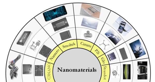
Perhaps you already have a smartphone which is water repellent. Then you maybe already reaping the benefits of a product made out of nanomaterials! P2i is a nanomaterial company that has figured out a way to convert molecules into water repellent nanomaterials coating! They already have shipped 250+ Millions of devices including smartphones, headphones, Bluetooth headsets and hearing aids protected through their nanomaterial technology.
Now, what could be the natural evolution of smartphone or gadgets in the coming years? Could it be flexible smartphone design that may win the consumer’s interest, or perhaps gadgets with even bendable or stretchable displays? Well then, C3NANO and Canatu are doing the right thing to bring such fantasy into reality;
C3NANO essentially glue or fuse silver nanowires at nanoscale making the materials enhancing both the transparency and the touch sensitivity performances.
Canatu bringing their proprietary Carbon NanoBud® material, which enable design freedom for touch interfaces with the ability to stretch the screen to more than 200%. Such carbon nanomaterials can be bent and flexed in tighter radii than 1 mm! Thanks to the involved carbon atoms which does not reflect any light, enables touch displays with deep black and high contrast. Maybe one day soon they will enable completely transparent monitors which were seen in sci-fi movies like in The Avengers a reality.
Then why to miss out the opportunity to enjoy the extremely detailed perfectly colored resolution in virtual reality (VR) experience? Hopefully we won’t, since Glo is bringing their heterogeneous nanomaterials technology to enable just that!
Transparent bendable display, and VR experience may be cool, but how often do we charge our smartphone? Would it be even more cool if we could charge our smartphone in less than 60 seconds? Storedot aims to empower exactly that. They are exploiting nanomaterials in the form of particles including silicon, carbon and some more elements to enable the quick charging.
Still, It’s the inside that counts
So far we have been talking about the outside of a smartphone. How about the inside of a smartphone, which essentially enables us to do so much of magic with our fingertips? No worries, we have that covered as well. Let’s highlight two essentials parts, or the brain if you will, of a smart gadget like smartphone: (a) the App processor and (b) the memory. The more artificial intelligence (AI), augmented reality (AR) and virtual reality (VR) we would like to experience, the better these two guys need to be in the form of computational power, memory bandwidth and power efficiency.
Nantero is bringing carbon nanotubes to build high-density non-volatile memory called NRAM® that is incredibly fast, can deliver the potential for terabits of storage in a single chip while consuming very little power. If you suddenly got 10x faster memory in your next gadget, don’t get surprised, it may be from them.
Now what about the App processor? The App microprocessor does the really hard job (the computational work) to enable an app to run a function through our fingertips. Moreover, the rise of AI, and greater demands for AR, VR and many other functionalities, the App microprocessor needs to work terribly hard to coup up with the computational power demand. To get into a slightly deeper inside of the app processor, such spiky power demands are staggeringly high that stresses the corresponding circuit power management to malfunction. Such event can lead to slow pace in the app to function or worse case hiccups or even shutdown of the processor!
Smoltek technology will fulfill such high paced demand for power bank at a very small footprint. It’s CNF-MIM technology exploits carbon nanofibers materials to build such power bank in the form of high value capacitors which can be placed directly inside and around an App processor to tackle such power surge so that the mammoth orchestra of computational work can run smoothly without a hiccup.
The beauty of Smoltek’s CNF-MIM capacitors is enabling a 3D surface area in a 2D footprint! Smoltek however is not satisfied with just that, but also want to bring the benefits of carbon nanomaterials even for 2.5D and 3D advanced packaging and heterogeneous integration solutions, so that more complex, embedded and power hungry systems can be assembled together at a smaller, slicker footprint.
To sum up, some technology is taking longer than other but the picture is converging to bring products to market. Everyone have their own way of exploiting the properties of nanomaterials for good. The difference is made in the innovative approaches and it is all about paying attention to the details. For nanomaterials case such attention has happened to be down to the nano level or even perhaps atomic level. Understanding of different mechanisms behind what matters and what not at that level creates the opportunity for innovations to improve the functions/properties of a device.
The definitive areas where the nanomaterials impacting are: smaller, faster, performance enhancement, embedded functionality, light-weight, eco-friendly and of course more for the buck.
Smoltek, the company once I have started and lived through and witnessing how barriers are broken in many different perspectives. The journey started with a tiny little idea of a product on making a sensor based on grown carbon nanomaterials. The initial idea didn’t fly in the industry obviously due to a technical issue or even a bottleneck: the temperature to grow these nanomaterials is so high that it would kill other devices.
We took a pivot at that point to focus and solve that particular temperature problem. Through many years of R&D, the team have figured out a few engineering nobs that can be played with to tune processes to enable growing carbon nanostructures on a given surface. The surface can be anything, including aluminium foil from our kitchen! Smoltek’s main breakthrough came when we found the sweet spot to grow carbon nanofibers at a temperature below 390 °C.
Breakthrough in growing the carbon nanomaterials at below 390°C, an industry compatible temperature, also have broken the hardest technical barrier.
This is the border line for CMOS industry, the industry that makes up the digital world as of today. From this point on industrial application can take off.
At this stage we were only welcomed by the industry but yet to be wanted. Now we had to proof what our nanomaterial growth technology could be good for. Another barrier popped up: Finding a pain point for industry where our materials fit to release the pain becomes the next barrier to break. And we found one, the capacitor!
The unbeatable form factor and 10–100× smaller footprint compared to existing technology opens up the door to disrupt (replace) existing technology in many technology verticals. What Smoltek is building in terms of capacitor, in generic terms can be considered as an energy storage bank. We can store tremendous amount of charge within a very small footprint. Freeing out important and expensive real-estate area on a silicon chip or a PCB. Today, company is gearing up its activities together with industrial players to bring the technology into product(s).
The capacitor is one of the fundamental building blocks for any given circuit. It is used for many reasons. One of the most essential use of them is to be used for managing power glitches that may occur during the switching events of billions of transistors. Such a gigantic orchestra is typically harmonized through using capacitors at different levels of circuits so the music can be played out without a hitch.
The high value capacitors can then find its way inside high performing microprocessors for AR, VR, AI, smartphones, cloud computing, tablets, laptops, wearables, heterogeneous integration and eventually any other internet of things (IoT) inspired electronic devices or gadgets.
The reason behind why Smoltek’s capacitor device is so cool is due to the versatility of its form factor! Depending on the demand of an application, the form factors can be changed to boosted up the energy storage capacity. For internet of things, power management will be essential at a very small footprint.
Introduction of AI into the Smartphone have started and demand will continue to enable performing local AI tasks without being in connecting with the cloud. VR and AR will also hit the road to create tremendous load on the power management of individual processors. To make them functioning without a power glitch, the capacitor banks will act as the savior of the day.
The potential of Nanomaterials technology enables such deeply rooted technology that every sector of the hardware platform is bound to be benefited when exploited appropriately. ‘Less is more’ perhaps a perfect way of summarizing about the nanomaterials. We have reached to an inflection point in technological progress where my take is, nanomaterials are no longer a choice, neither about disruptions, rather it is about inevitability to drive the future. The existing hardware platform and software have brought the world within our thumb. I wonder what our thumb will be empowered to do when the fusion of nanomaterials and nanotechnology is realized. Something worth watching for.
Whatever direction the future gadgets will take, we have it all covered through nanomaterials and nanotechnology. After over a decade of witnessing the shift from being only hype to reality, creating paths which did not exist, it is indeed a very strange mix of inexpressibly touchy feelings to observe that things are suddenly aligning in order. Industrial interest increasing from day to day to come up integration possibilities not only towards our own envisioned application but also for the customer’s own identified applications.
Such an entrepreneurial journey would have not been possible without the system that supports it and the people supporting such endeavors to stay in the course of development. The team, and the investors all have shown tremendous entrepreneurial stamina to come to this far. It is once again showing the case that the entrepreneurs do not take ‘no’ for an answer. And the word ‘failure’ do not exists in their dictionary.
I however have realized that I am only getting warmed up and ready to shift my gear to bring the future to the reality through accelerated innovations and industrialization. We surely have more barriers to break. Such barriers however do not concern me since it is in our nature to breaking barriers!
The journey in bringing the nanomaterials to the society evidently creating more opportunities for investors, create more jobs for highly talented people and not but least more super smart gadgets to enjoy the life for ourselves and for the generation to come. Visualizing such scenario, I am feeling a hidden pleasure of my vision of turning a simple idea into societal values to be a reality. Such feelings make me to wake up every morning and go to work and drives me to do what I do.
ICYMI: The previous article in the series: Breaking Barriers, part II: The Reality, and of course the first article in the series: Breaking Barriers, part I: The Hype.
Your data will be handled in compliance with our privacy policy.
IR Blog Posts
January 9, 2025
Modern electronics demand increasingly compact and powerful capacitors, and the race for miniaturization has reached a critical juncture. While both Deep Trench Capacitors (DTC) and Carbon Nanofiber Metal-Insulator-Metal (CNF-MIM) capacitors are being developed for advanced applications requiring smaller size and higher capacitance density than conventional surface-mounted capacitors, DTC pushes the boundaries of what’s achievable with subtractive manufacturing, but is hitting fundamental physical limits. In contrast, Smoltek’s innovative CNF-MIM technology offers a revolutionary path forward, unrestricted by these constraints.
IR Blog Posts
December 20, 2024
An interview with Smoltek Hydrogen CEO Ellinor Ehrnberg about her recent visit to Germany and the rapid acceleration of the hydrogen economy.
IR Blog Posts

February 27, 2025
In an age where environmental sustainability is of utter importance, it is crucial to find innovative solutions to reduce energy consumption and minimize our carbon footprint. One such solution is found in capacitors. These unassuming electronic components not only play an important role in various systems, but also offer significant environmental benefits. Albeit very small – if counted one by one.
IR Blog Posts

December 10, 2024
The ultra-thin capacitor market is entering a new phase as major players like Murata and Samsung invest heavily in silicon-based solutions. In a recent interview, YAGEO Group's CTO Philip Lessner explains why Smoltek's CNF-MIM technology could offer superior advantages to silicon-based solutions in this rapidly growing market.
IR Blog Posts

November 20, 2025
In the first ”Smoltalk” podcast, CEO Magnus Andersson is joined by Smoltek Semi CTO Dr. Farzan Ghavanini for a technical deep dive. Dr. Ghavanini discusses the core CNF-MIM technology in detail, covering everything from its unique material properties and AI applications to the complete product roadmap, key partnerships, and future integration plans. This article summarize the highlights of the conversation.
IR Blog Posts
October 29, 2025
At the Hydrogen Technology World Expo 2025 in Hamburg, Ellinor Ehrnberg, President of Smoltek Hydrogen, joined a high-level panel to debate one of the industry’s most pressing challenges: How can green hydrogen be scaled fast enough—and affordably enough—to meet the world’s decarbonization goals?