Sign up for our newsletter!
Your data will be handled in compliance with our privacy policy.
Your data will be handled in compliance with our privacy policy.


In the first ”Smoltalk” podcast, CEO Magnus Andersson is joined by Smoltek Semi CTO Dr. Farzan Ghavanini for a technical deep dive. Dr. Ghavanini discusses the core CNF-MIM technology in detail, covering everything from its unique material properties and AI applications to the complete product roadmap, key partnerships, and future integration plans. This article summarize the highlights of the conversation.
Thomas Barregren • November 20, 2025
In the premiere episode of the new podcast, Smoltalk, Smoltek CEO Magnus Andersson sits down with Smoltek CTO Dr. Farzan Ghavanini to talk about Smoltek Semi’s ultra-thin capacitors, called CNF-MIM, and the technology and business behind them. The episode is available on Apple Podcasts, Spotify, and most other podcast directories, as well as on YouTube. Below is a summary of the discussion between the two gentlemen.
The company is approaching its 20th anniversary, a significant achievement for a development-phase company. Dr. Ghavanini notes that the original founders, including Shafiq and Professor Peter Enoksson, are still actively involved as employees or shareholders. Andersson sees this long-term commitment as a “testament to the potential” of the core technology.
Smoltek’s carbon nanofibers (CNF) possess a unique combination of three key properties. They are excellent conductors of electricity, excellent conductors of heat, and, as nanostructures, they have an extremely high surface-to-volume ratio.
It is this massive surface area (or “high aspect ratio”) that both Smoltek Semi (for capacitors) and Smoltek Hydrogen (for electrolyzers) leverage to build components that are far more efficient and compact than traditional solutions.
Smoltek Semi focuses on an emerging class of “ultra-thin capacitors.” These are not conventional components like MLCCs (which are 300–400 micrometers thick) but are instead fabricated using advanced semiconductor processes.
This allows for components well below 100 micrometers. Dr. Ghavanini confirms that Smoltek has already successfully demonstrated capacitors as thin as 40 micrometers.
This ultra-thin profile is critical for the AI revolution. Advanced AI processors, like NVIDIA’s H100, experience massive transient currents, drawing hundreds of amps in mere nanoseconds. To function, they need a large “reservoir of electrons” (a capacitor) available instantly.
This requires two things: high capacitance density and extreme proximity to the processor. Smoltek’s technology is engineered to deliver both, solving the “power delivery dilemma” that is a major bottleneck for AI hardware.
While artificial intelligence (AI) and high-performance computing (HPC) are the primary drivers, the technology is also perfectly suited for other space-constrained applications. These include wearables like smartwatches and earpods.
Furthermore, the technology is ideal for high-frequency (RF) applications. In RF systems, components must be very small to match the transmission lines, preventing signal reflections and energy waste.
Today, the main competitor in the ultra-thin space is silicon trench technology. Dr. Ghavanini explains the key difference. Trench technology etches deep, narrow trenches into silicon, achieving an aspect ratio (depth-to-width) of about 20–25. To get enough capacitance, they must stack multiple capacitor layers inside these trenches.
Each layer requires a costly and slow manufacturing step called Atomic Layer Deposition (ALD). Stacking four layers means paying for that expensive process four times.
Smoltek’s CNF-MIM technology grows nanofibers with an aspect ratio of 100 (for Gen-One). Because this ratio is so high, Smoltek can achieve comparable performance with just one ALD step, creating a fundamental cost advantage and a new “S‑curve” for innovation by simply growing the fibers taller.
Smoltek is now in the “lab-to-fab” phase, which is focused on industrialization. As a unique technology, Dr. Ghavanini notes that the “burden of proof” is high. The most important milestone is proving reliability.
Smoltek recently announced a major success on this front: its capacitors passed a 1,000-hour test at 85°C. This proves that the technology is “fundamentally reliable,” a critical step toward commercialization. The next phase is focused on producing customer validation samples of Gen-One.
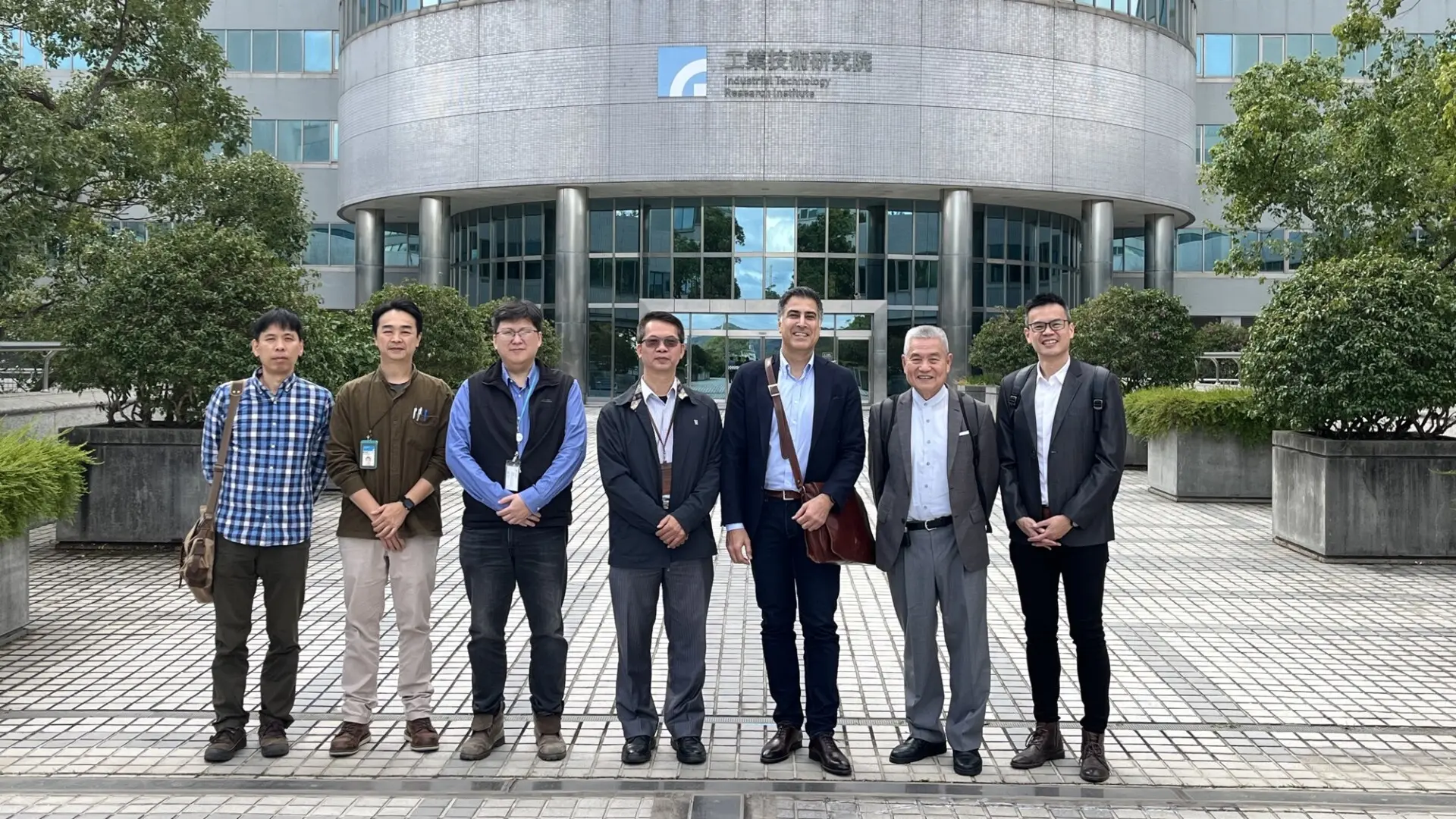
This progress is supported by key partners. The Industrial Technology Research Institute (ITRI) in Taiwan, a world-renowned semiconductor institute, is a crucial partner on two fronts. First, ITRI is fabricating the “Gen-One” validation samples. Second, they are collaborating with Smoltek to establish a “pilot line” for low-volume production, providing powerful external validation for the Asian market.
Smoltek also maintains a strong technical collaboration with YAGEO and its subsidiary, Kemet, with monthly technical meetings. This partnership provides expert validation and access to specialized equipment.
For example, YAGEO/Kemet helped simulate the capacitor’s parasitic inductance (ESL), which was calculated to be around one picohenry—an excellent result that is too low for Smoltek to even measure with its own equipment.
With a new, in-house ALD system, Smoltek will accelerate its R&D and IP generation. The future roadmap includes “Gen-Two” trough “Gen-Three,” which will feature even taller fibers for higher capacitance.
The go-to-market plan starts with a standalone, discrete capacitor. This will be followed by advanced integration, such as embedding the capacitor into an interposer. The long-term vision is to grow nanofibers directly onto the active CMOS chip (backend of line), achieving the closest possible integration.
This integration strategy aligns perfectly with the “chiplet” trend, which involves breaking large processors into smaller, specialized components. Smoltek is part Chips Joint Undertaking (Chips JU). In this ecosystem, Smoltek’s capacitor-on-silicon would function as a specialized chiplet dedicated to power distribution, solving a key challenge for next-generation hardware.
This article covers the main topics from the premiere episode of Smoltalk. To hear the full, in-depth conversation with Dr. Farzan Ghavanini, listen to the full episode.
You find Smoltalk on Apple Podcasts, Spotify, and most other podcast directories, as well as on YouTube.
Your data will be handled in compliance with our privacy policy.
IR Blog Posts

January 9, 2025
Modern electronics demand increasingly compact and powerful capacitors, and the race for miniaturization has reached a critical juncture. While both Deep Trench Capacitors (DTC) and Carbon Nanofiber Metal-Insulator-Metal (CNF-MIM) capacitors are being developed for advanced applications requiring smaller size and higher capacitance density than conventional surface-mounted capacitors, DTC pushes the boundaries of what’s achievable with subtractive manufacturing, but is hitting fundamental physical limits. In contrast, Smoltek’s innovative CNF-MIM technology offers a revolutionary path forward, unrestricted by these constraints.
IR Blog Posts

April 14, 2025
Taking a breakthrough technology from the lab bench to the world market often requires collaboration with large industrial enterprises. In this interview, Ellinor Ehrnberg, president of Smoltek Hydrogen, explains how the company aligns its own development with that of potential buyers while navigating the complex journey from initial interest to strategic partnership.
IR Blog Posts

July 30, 2025
The recently signed technical service agreement between Smoltek Semi and the Industrial Technology Research Institute (ITRI) of Taiwan changes how CNF-MIM capacitors will reach the market. This partnership delivers the validation and manufacturing capabilities needed to transform laboratory breakthroughs into commercial reality.
IR Blog Posts

February 27, 2025
In an age where environmental sustainability is of utter importance, it is crucial to find innovative solutions to reduce energy consumption and minimize our carbon footprint. One such solution is found in capacitors. These unassuming electronic components not only play an important role in various systems, but also offer significant environmental benefits. Albeit very small – if counted one by one.
News
June 18, 2025
Smoltek Semi has initiated the signing of a technical service agreement with the Taiwanese Industrial Technology Research Institute (ITRI) that enables low-volume production of Smoltek's propriety CNF-MIM capacitors.
IR Blog Posts

June 16, 2025
Smoltek Semi joins an elite club of companies achieving 1 µF/mm² capacitance density, but stands alone in reaching this milestone with an ultra-thin profile. This breakthrough unlocks the under-chip real estate that represents the holy grail of capacitor placement in modern electronics.