Sign up for our newsletter!
Your data will be handled in compliance with our privacy policy.
Your data will be handled in compliance with our privacy policy.

Research paper published in the proceedings of 2018 IEEE 68th Electronic Components and Technology Conference (ECTC), 2018, pp. 2313-2318.
R Andersson, A M Saleem, V Desmaris • August 9, 2018
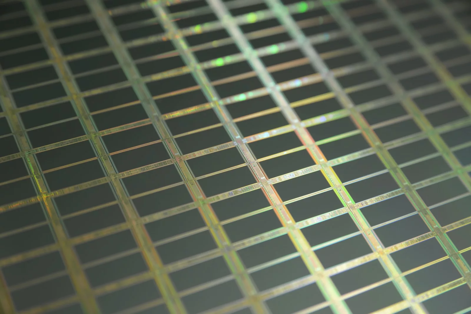
Complete on-chip fully solid-state 3D integrated capacitors using vertically aligned carbon nanofibers as electrodes to provide a large 3D surface in a MIM configuration have been manufactured and characterized in terms of capacitance per device footprint area. The fibers are grown directly on the bottom electrode surface and then conformally coated with a dielectric material using atomic layer deposition. Two different dielectric materials, Al2O3 and HfO2 , of different thicknesses have been investigated, and different constructions for the top electrode have been tested. The entire manufacturing process is completely CMOS compatible, which along with the low device profile of about 4 μm makes the devices readily available for integration on a CMOS-chip, in 3D stacking, or in a 2.5D interposer technology. Capacitance values of up to 18.2 nF/mm2 (per device footprint area) are achieved reproducibly.
Your data will be handled in compliance with our privacy policy.