Sign up for our newsletter!
Your data will be handled in compliance with our privacy policy.
Your data will be handled in compliance with our privacy policy.

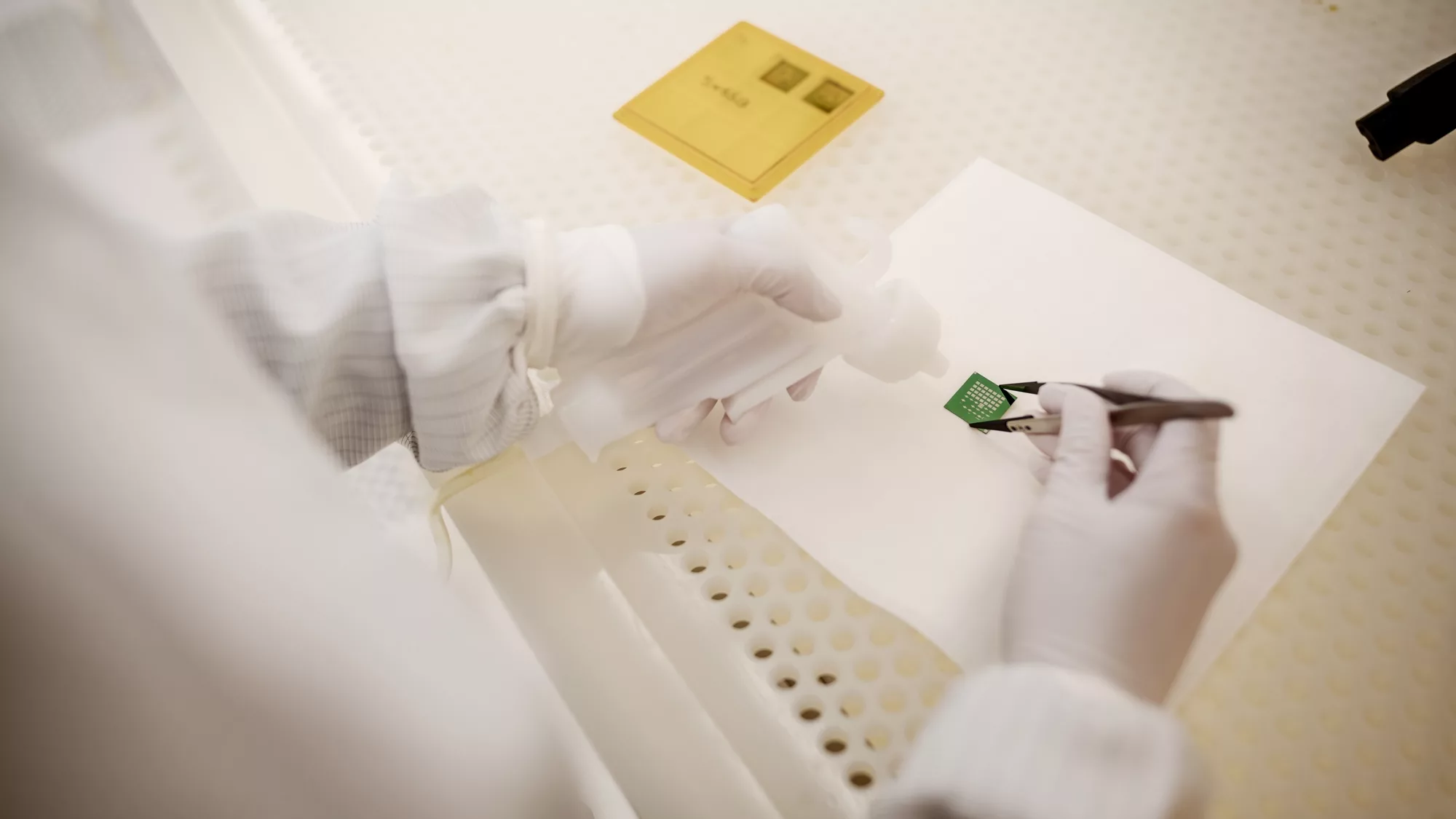
Smoltek Semi has developed a new process, known as zapping, that reduces the number of steps required to manufacture test capacitors.
The new zapping method cuts the time to manufacture test capacitors from nearly a month to just one week. The faster manufacturing process enables Smoltek’s researchers to conduct more experiments that accelerate major technology advances – making the CNF-MIM technology more attractive to potential buyers.
By cutting the development time so dramatically, we can iterate faster and focus more on optimizing performance. This efficiency allows us to explore new configurations and achieve breakthroughs much sooner, which strengthens our position when engaging with potential buyers.
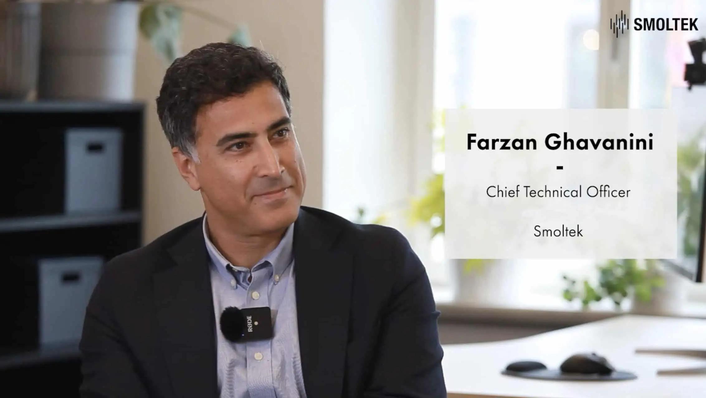
Farzan Ghavanini, CTO at Smoltek.
The new method, called zapping, is exclusively used during the development phase to expedite testing. It enables researchers to quickly evaluate new configurations and materials using simplified test capacitors, saving valuable time and resources.
Zapping is a clear advantage for us and our shareholders. Faster development cycles mean shorter time to market for breakthroughs, like tripling capacitance density and halving leakage current.
Farzan Ghavanini
Zapping, explained:
The zapping method involves briefly applying a high voltage across specific contact points on a test capacitor, creating a controlled breakdown in the insulating layer. This technique eliminates the need for multiple complex etching steps, significantly streamlining the testing process.
For a more detailed explanation of the zapping method and its impact on Smoltek’s capacitor technology development, please visit the company’s IR blog.
Your data will be handled in compliance with our privacy policy.
News
February 24, 2026
An independent, third-party reliability test of our CNF-MIM capacitor technology has confirmed the reliability results communicated on February 5, 2026. The independent validation, performed by a major capacitor manufacturer, also reduces technical risk in the commercialization process and strengthens Smoltek’s credibility in ongoing negotiations with industrial partners.
News

February 5, 2026
Smoltek’s CNF-MIM capacitors demonstrate excellent stability in a new 1,000-hour life test at 85°C under applied 2 volts. No degradations were observed, and the capacitors exhibited more than 1,000 times lower current leakage compared to the previous life test.
News

November 20, 2025
We have launched a podcast about materials technology and investments in general and our disruptive carbon nanotechnology in particular.
News
November 17, 2025
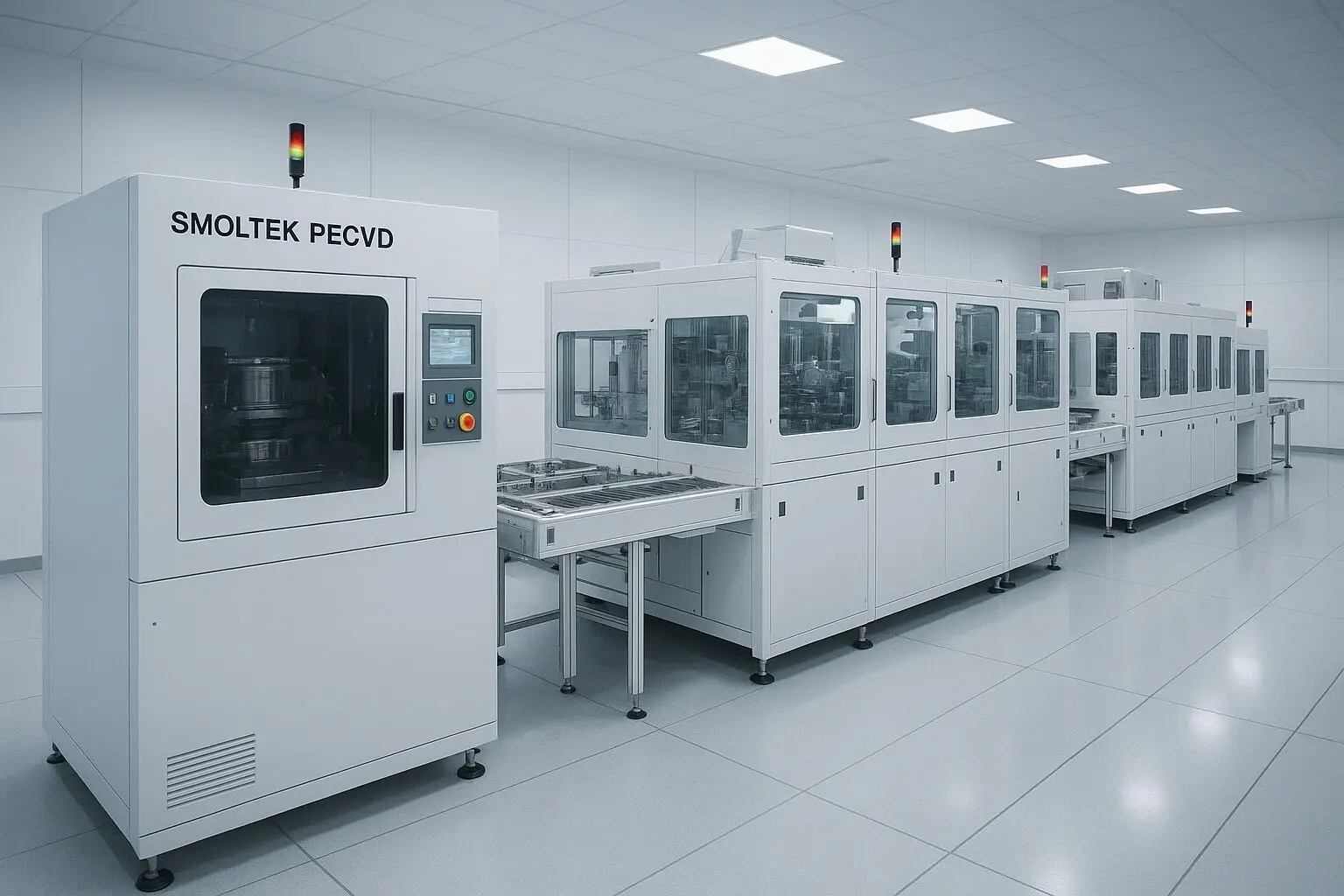
Smoltek Semi is currently optimizing the company’s advanced PECVD system to ensure implementation of its most recent technological innovations in CNF synthesis, enabling compliance with stringent customer requirements, prior to installation at ITRI in Taiwan.
News

November 5, 2025
Smoltek Semi has reached an important technical milestone in the development of the company’s carbon fiber-based CNF-MIM technology. The capacitors have successfully passed a 1,000-hour high-temperature durability test, confirming the robustness of the technology for advanced applications.
News

October 24, 2025
Smoltek Semi has acquired a plasma-enhanced Atomic Layer Deposition (ALD) system to implement its advanced dielectric stack on carbon nanofibers. The system will significantly reduce the iteration time of coating processes while enabling innovation and IP generation in dielectric stack technology for carbon nanofiber electrodes.