Sign up for our newsletter!
Your data will be handled in compliance with our privacy policy.
Your data will be handled in compliance with our privacy policy.


Smoltek Semi joins an elite club of companies achieving 1 µF/mm² capacitance density, but stands alone in reaching this milestone with an ultra-thin profile. This breakthrough unlocks the under-chip real estate that represents the holy grail of capacitor placement in modern electronics.
Thomas Barregren • June 16, 2025
Smoltek Semi has achieved 1 µF (one microfarad) of capacitance on an area measuring just one square millimeter. This represents a dramatic leap from nanofarad to microfarad territory – a threshold that seemed almost mythical just years ago for ultra-thin integrated capacitors. While we’re not the first to cross this coveted line – a few other companies have achieved this prestigious milestone in the specialized field of ultra-thin capacitor technologies – our accomplishment sets us apart in this exclusive club. We reached 1 µF/mm² while keeping our capacitor incredibly thin, unlocking possibilities that others simply cannot match.
Today’s smartphones pack more computing power than room-sized supercomputers from decades past. High-performance computing (HPC) centers and AI accelerators push processing speeds to extraordinary limits. But this performance comes with a fundamental challenge: as chips become faster, they become more demanding about their power supply.
Think of transistors as incredibly fast switches, flipping billions of times per second between ones and zeros. Each flip demands instant energy, creating power fluctuations that would cripple performance without intervention. Capacitors serve as lightning-fast energy reservoirs, absorbing excess power and releasing stored energy precisely when needed.
The closer these capacitors sit to the chip, the better they perform. Distance means delay, and delay means degraded performance. The ultimate proximity lies directly under the chip, nestled between the solder balls that connect the processor to the circuit board. But this prime real estate comes with a merciless constraint: height.
Here’s where most solutions hit their limitation wall. Achieving 1 µF/mm² while fitting under solder balls demands an ultra-thin profile. The solder balls themselves define the height limit – typically allowing only minimal clearance for integrated components.
Smoltek has cracked this code with a capacitor featuring an active layer of just 6 µm. To put this in perspective, a human hair measures about 70 µm in diameter. Smoltek’s active capacitor layer could fit more than ten times under the width of a single hair. This isn’t just thin – it’s what engineers call ”truly ultra-thin” for the critical performance area.
This achievement transforms Smoltek from another member of the 1 µF/mm² club into the only company capable of delivering that performance where it matters most: in the space-constrained under-chip environment where every micrometer counts.
Understanding Smoltek’s breakthrough requires grasping how CNF-MIM capacitors work. Deep Trench Capacitors (DTC) carve deep trenches – like miniature wells – in a silicon substrate. In contrast, CNF-MIM manufacturing takes a fundamentally different approach by growing forests of carbon nanofibers on a substrate. Picture microscopic trees, each about 10,000 times thinner than human hair, standing vertically in dense formation.
The magic happens in the layering process. Each carbon nanofiber gets coated with metal, applied atom by atom using Atomic Layer Deposition (ALD). Over this metal layer, Smoltek applies our proprietary ZrO₂–Al₂O₃ dielectric stack – again, atom by atom with atomic precision. Finally, another metal layer completes the structure, creating a metal-insulator-metal capacitor at nanoscale.
This atom-by-atom construction allows Smoltek to utilize 100% of the surface area provided by the carbon nanofibers. No other deposition method achieves this complete coverage, making ALD essential for maximizing capacitance density.
The precision ALD processes that make CNF-MIM possible require specialized equipment at industrial scale. Smoltek has partnered with SkyTech, a Taiwanese leader in ALD equipment for the semiconductor industry.
The partnership gives Smoltek access to the same industrial-scale deposition technology used throughout semiconductor manufacturing. SkyTech’s expertise ensures our processes maintain their performance characteristics as they transition from laboratory to mass production.
Most importantly, the collaboration proves real-world scalability. Once the processes are fully developed, scaling up for mass production becomes straightforward. This isn’t laboratory innovation that might work someday – it’s production-ready technology with a clear path to market.
Beyond superior performance, CNF-MIM technology delivers compelling economics. While competing technologies, such as DTC, demand multiple expensive ALD processes to achieve similar results, Smoltek’s approach requires significantly fewer layers – directly translating to lower production costs.
ALD represents one of the most expensive processes in semiconductor manufacturing. Since CNF technology can achieve the same capacitance with fewer ALD layers compared to deep trench alternatives, the cost advantage compounds with each performance increment. This isn’t just about better technology – it’s about better technology that costs less to produce.
The economic implications are profound: as performance requirements increase, traditional approaches see exponential cost growth, while CNF-MIM maintains cost efficiency through its superior three-dimensional architecture.
These results aren’t laboratory curiosities achieved under perfect conditions. The majority of tested devices showed consistent capacitance density with reliable reproducibility – the hallmark of mature technology ready for commercialization.
While current data comes from simplified CNF-MIM devices in laboratory settings, the same dielectric stack produces prototypes and products achieving identical performance. The 18-month development process has created production-ready processes that translate directly to commercial manufacturing.
Development focus has now shifted to improving insulation resistance – essential for minimizing leakage current and ensuring long-term reliability in commercial applications.
The significance of Smoltek’s achievement extends beyond technical metrics. In a recent interview, leading capacitor manufacturer Yageo acknowledged the groundbreaking capabilities of CNF-MIM technology.
This industry validation confirms what the technical data suggests: Smoltek has developed something genuinely unique in the capacitor industry. Expert recognition from a major industry player underscores the commercial potential of a technology that solves problems others cannot even address.
Every smartphone, AI accelerator, and HPC processor requires capacitors for power stabilization. Physics dictates that closer placement means better performance, and under-chip real estate offers the ultimate proximity. Yet until now, no technology could deliver meaningful capacitance in this space while meeting height constraints.
Smoltek has solved this equation. We’ve joined the exclusive 1 µF/mm² club while standing alone in our ability to achieve this performance with ultra-thin profiles. As electronics continue their relentless march toward higher performance in smaller packages, this unique capability transforms from technical curiosity to commercial necessity.
The path from laboratory breakthrough to market dominance runs through problems that only one company can solve. For investors seeking exposure to technologies that address seemingly impossible constraints, Smoltek offers capabilities that literally don’t exist anywhere else.
Your data will be handled in compliance with our privacy policy.
IR Blog Posts

January 9, 2025
Modern electronics demand increasingly compact and powerful capacitors, and the race for miniaturization has reached a critical juncture. While both Deep Trench Capacitors (DTC) and Carbon Nanofiber Metal-Insulator-Metal (CNF-MIM) capacitors are being developed for advanced applications requiring smaller size and higher capacitance density than conventional surface-mounted capacitors, DTC pushes the boundaries of what’s achievable with subtractive manufacturing, but is hitting fundamental physical limits. In contrast, Smoltek’s innovative CNF-MIM technology offers a revolutionary path forward, unrestricted by these constraints.
IR Blog Posts

October 1, 2024
Smoltek Semi has developed a new material for use in CNF-MIM capacitors. The new material increases capacitance by more than three times and reduces leakage current by 50 percent. In this article, we examine what this means and why it is good for shareholders and investors.
IR Blog Posts

September 5, 2024
Smoltek’s focus on qualified research places it firmly in the Explorer quadrant of the R&D Evaluation Matrix, a model for assessing a company’s research and development strategy. Discover why this matters to investors and how Smoltek translates groundbreaking research into valuable business opportunities.
News
June 18, 2025
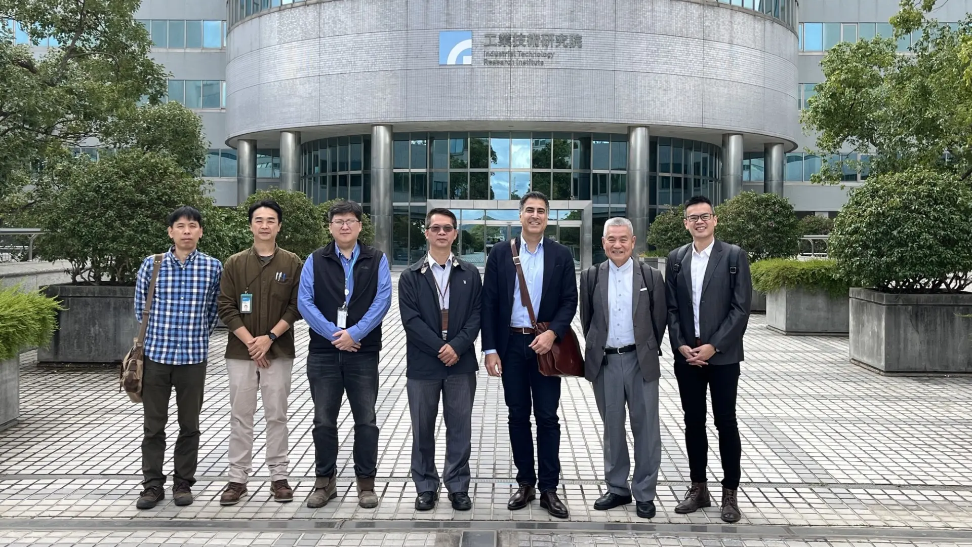
Smoltek Semi has initiated the signing of a technical service agreement with the Taiwanese Industrial Technology Research Institute (ITRI) that enables low-volume production of Smoltek's propriety CNF-MIM capacitors.
News

September 13, 2024
Smoltek is a Gothenburg-based materials technology company that specializes in research and development of applications based on carbon nanofibers, which can create new products with revolutionary properties.
IR Blog Posts

October 11, 2024
Our innovative “zapping” method drastically reduces development time and costs, enabling us to advance CNF-MIM technology faster and making Smoltek Semi’s technology even more attractive to potential buyers. Read on to see how this new process strengthens our position and shortens our path to market.