Sign up for our newsletter!
Your data will be handled in compliance with our privacy policy.
Your data will be handled in compliance with our privacy policy.

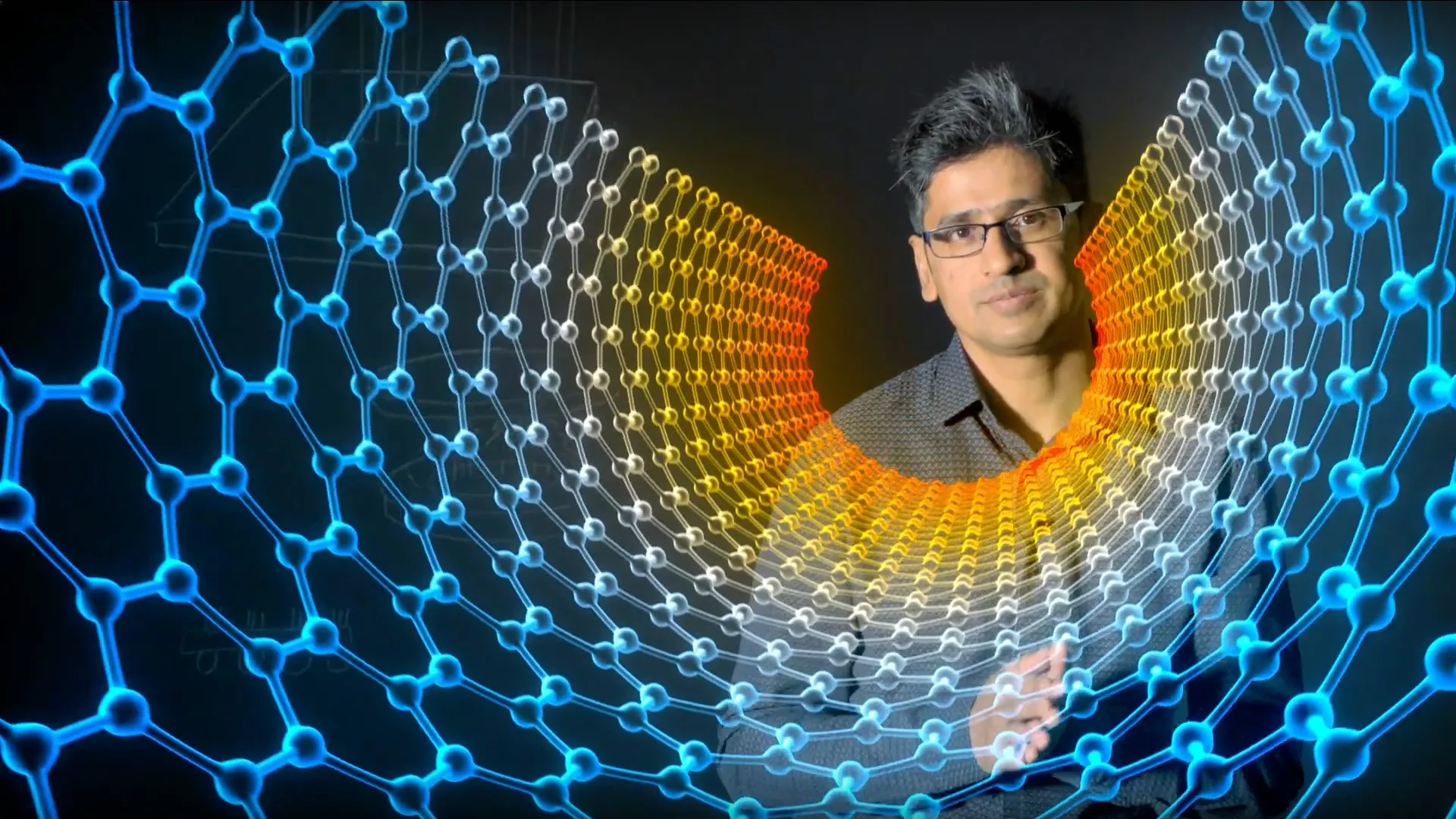
Smoltek conducts advanced research and innovation based on nanotechnology to develop new material technology opportunities that can solve many of today's industrial challenges. This journey began 20 years ago, when Dr. Shafiq Kabir, together with David Brudö and Dr. Peter Enoksson, founded the company.
Fredrik Liljeberg • December 12, 2025
Over two decades, Smoltek has developed from a research-driven deep tech company to an industrial player with groundbreaking nanotechnology for both semiconductors and hydrogen – validated by leading global partners and on its way to commercialization.
Much water has flowed under the bridge since the company was founded, and today Smoltek is developing a new generation of energy and cost-efficient capacitors for advanced chips in the semiconductor industry, as well as cost-saving electrodes for electrolyzers and fuel cells in the hydrogen industry.
But let’s take a trip down memory lane.
Here’s what Shafiq Kabir said about why he took the initiative to found the company back in December 2005:
“I founded the company out of scientific curiosity and with the ambition to develop technological solutions based on nanostructures that can be useful in many industrial areas. The reason was my ambition to drive my research results in nanotechnology to create new innovations for use in industry. By switching to research and development on a commercial basis, we wanted to make the possibilities of nanotechnology available on a much larger scale.
Since its inception, Smoltek has methodically built and patented a comprehensive technology platform based on catalytic growth of conductive nanostructures, with much of the component and application development focused on carbon nanofibers and their various properties – which have superior electrical, mechanical and thermal strength.
The technology increases the reaction surface for chemical and electrical processes on a substrate by several magnitudes and enables products that are significantly more compact, energy-efficient and cost-effective than conventional solutions.
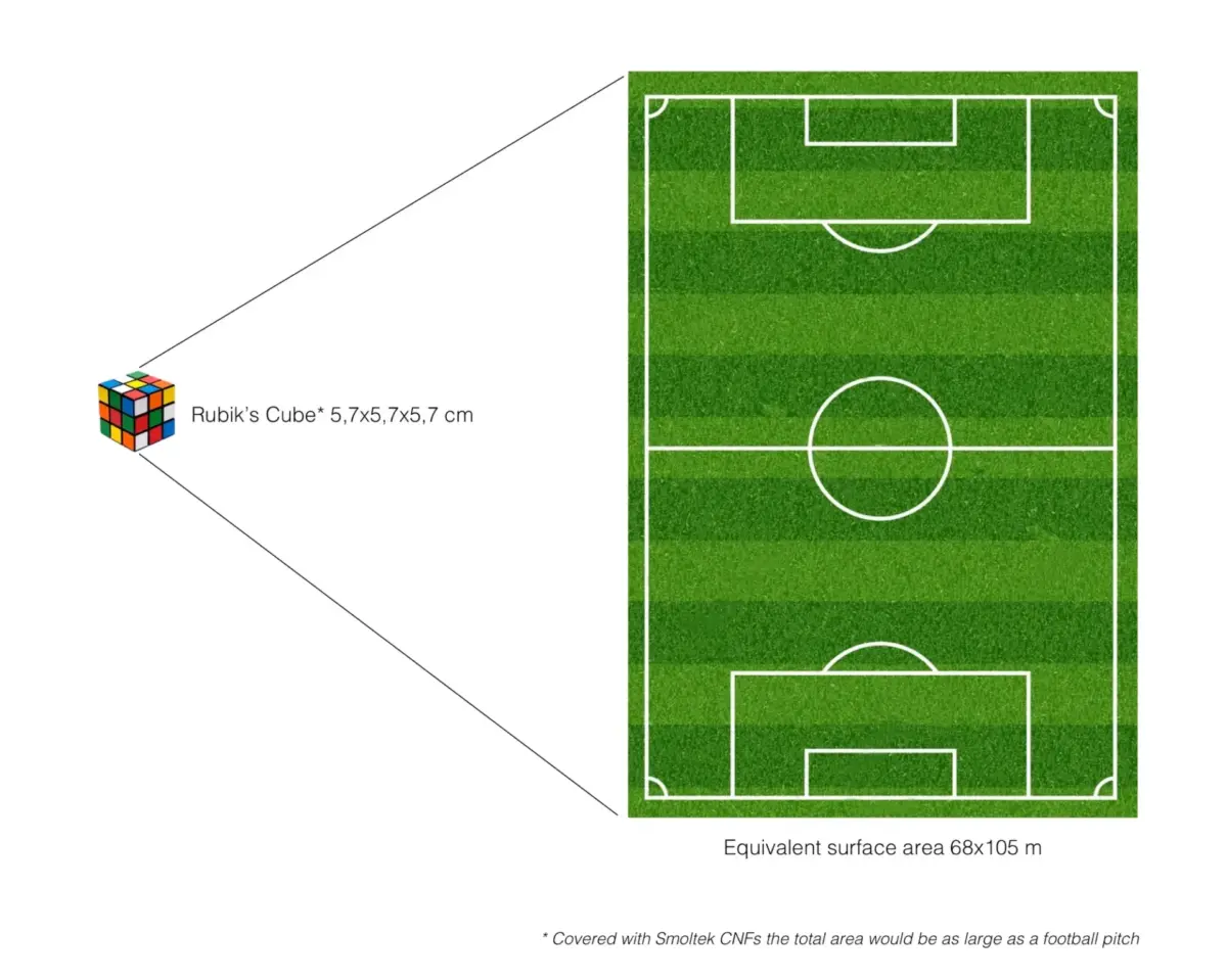
For instance, if you were to cover a Rubik’s Cube with Smoltek’s conductive carbon nanofibers, the available surface area for chemical and electrical processes would be as large as a football field. That is the great advantage of Smoltek’s carbon nanotechnology.
Smoltek has built up an extensive IP portfolio and gradually validated the technology. During the early years, the carbon growth process and the first prototypes in semiconductors were developed. Between 2012 and 2016, work was deepened towards semiconductor applications such as interconnects and integrated capacitors. The big breakthrough came in 2017 when the industry showed strong interest in Smoltek’s ultra-thin capacitor technology.
Today, Smoltek is a publicly traded company with three subsidiaries:
Smoltek develops applications based on nanotechnology to solve advanced material engineering challenges. By growing nanostructures directly on a material, the contact surface can be increased tens of thousands of times.
Properties of carbon nanofibers
Industrial technology areas possible for Smoltek’s nanotechnology
| Year | Milestone |
|---|---|
| 2005 | First core patent filed. |
| 2006 | Selective carbon nanofiber growth on silicon. |
| 2007 | Smoltek boosts the development activities at the MC2 laboratory at the Chalmers University of Technology. |
| 2008 | Carbon nanofiber growth on ASIC chip (an integrated circuit with a specific function). |
| 2009 | Patent platform in place, several patents filed. Carbon nanofiber growth on a silicon carbide device (SiC – a power module with a wide band gap that provides low coupling losses and high switching frequencies). |
| 2010 | First customer project, initiated from the CERN laboratory in Switzerland. Development of carbon nanofiber interconnects in an RF device (interconnected structures for regulating radio frequencies/oscillation rates of electromagnetic waves). |
| 2011 | Develops controlled growth of carbon nanofibers at only 390°C, meaning Smoltek has now achieved CMOS compatibility (industry standard in semiconductors). |
| 2012 | Significant increase in growth rate of carbon nanofibers in vacuum chamber. Obtains proof of CMOS compatibility (industry standard) for carbon growth concept. |
| 2013 | Intensification of R&D focus on capacitors. Agreement on industrial process development for growth of carbon nanofibers. |
| 2014 | First prototype of a supercapacitor (a chemical capacitor with very high capacitance that can store very high electrical charges) based on Smoltek’s carbon nanofibers developed. |
| 2015 | First prototype of an integrated carbon nanofiber-based capacitor (capacitor in an integrated circuit – protects the circuit from noise that can affect its performance and prevents the circuit from transmitting noise that can in turn affect the performance of other circuits) based on Smoltek’s carbon nanofibers developed. |
| 2016 | 3D electrodes based on Smoltek’s carbon nanofibers developed. |
| 2017 | The semiconductor industry is showing great interest in Smoltek’s capacitor technology, which can enable further miniaturization of chips while maintaining or improving performance. Smoltek Nanotech Holding AB is formed and the company is prepared for an IPO. |
| 2018 | Smotek Nanotech Holding AB is listed on Spotlight Stock Market in Stockholm, Sweden. The capacitance (per unit area) of our carbon-based (CNF-MIM) capacitors is doubled, making the technology very attractive to the semiconductor industry. |
| 2019 | Continuous progress with CNF-MIM technology. Capacitance is increased to 650 nF/square millimeter and internal resistance is kept below 40 mΩ, showing performance comparable to other solutions at a fraction of their build height. Smoltek Semi AB is formed, to handle licensing agreements with the semiconductor industry. |
| 2020 | Smoltek Semi sings a license agreements for the evaluation of the CNF-MIM technology. Smoltek Innovation (Hydrogen) AB is formed as a new subsidiary to bring Smoltek’s revolutionizing nanotechnology to new markets. The main area is the hydrogen industry, where our technology can be used for energy conversion and energy storage. |
| 2021 | Smoltek Semi manufactures the “world’s thinnest capacitor” – a prototype of a fully functional CNF-MIM capacitor with a total height of 38.2 µm (including the necessary substrate). Smoltek Hydrogen has focus on Proof-of-Concept testing of a new nanofiber-based cell material for PEM electrolyzers. |
| 2022 | Smoltek Semi signs a Joint Development Agreement with global capacitor giant Yageo group to commercialize ultra-thin decoupling capacitors for application processors. Smoltek Hydrogen signs a collaboration agreement with an international manufacturer of advanced materials for electrolyzers. This includes the joint construction of PEM electrolyzer cell prototypes to show that the performance significantly improves with our carbon nanofibers. |
| 2023 | Smoltek Semi develops a manufacturing process for 8‑inch wafers intended to produce industrially manufactured CNF-MIM capacitor prototypes in high volumes. Smoltek Hydrogen shows that the carbon nanofiber-based electrode for electrolyzers produces as much hydrogen with only 0.5 mg of iridium per square centimeter as a commercial standard material with 2.5 mg of iridium per square centimeter. |
| 2024 | Smotek Semi takes a major step forward in the development of CNF-MIM capacitor technology by introducing Gen-Zero – a new way to build high capacitance capacitors in a small footprint. This allows Smoltek to create a volumetric capacitance density of up to 120 nanofarads per square millimeter and per micrometer of nanofiber. Smoltek Hydrogen proves, in a 1,000-hour durability test, that the PTE (porous transport electrode) technology can produce hydrogen with a catalyst load of only 0,2 mg Iridium per square centimeter. The PTE technology is also validated by Dr. Felix Büchi, a highly regarded expert on PEM electrolysis. |
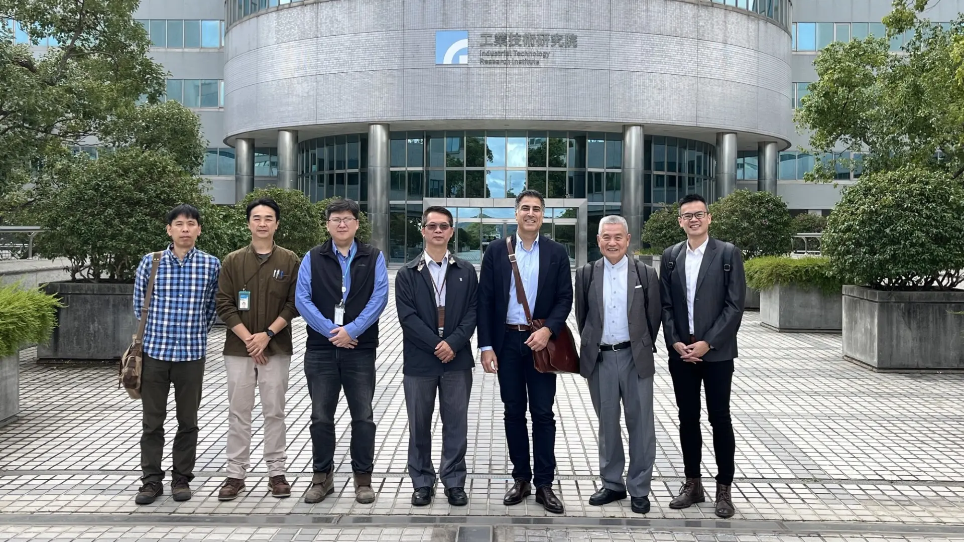
| 2025 | Smoltek Semi signs a technical service agreement with Taiwan’s Industrial Technology Research Institute (ITRI) for small-scale production of CNF-MIM capacitors. The agreement enables low-volume production of CNF-MIM capacitors, both industrially manufactured prototypes for customer tests and industrialized capacitors in smaller volumes for specialized customer projects. During the year, the CNF-MIM technology has successfully passed a 1,000-hour high-temperature durability test, confirming the robustness of the technology for advanced applications. Smoltek Hydrogen and Heraeus Precious Metals are initiating a joint development project in hydrogen technology to develop low iridium PTE electrodes (Porous Transport Electrode) for PEM electrolyzers. The company is also initiating a strategic collaboration with Impact Coatings with the ambition to jointly evaluate the possibilities of industrializing and scaling up Smoltek’s patented carbon nanofiber (CNF) technology for use in, among other things, PEM electrolyzers and fuel cells. |
Two decades of pioneering research and IP development have laid the foundation for Smoltek’s next phase—commercializing advanced nanotechnology solutions for the semiconductor and green-energy industries.
“Looking ahead, we see enormous potential in applying our nanotechnology to real-world problems. Everything we have learned—from the earliest experiments to today’s industrial collaborations—has prepared us for this moment. We are entering a phase where technology, market need, and capability align.”
Dr. Shafiq Kabir, founder and VP Volume Processes at Smoltek Hydrogen.
Read the official press release about Smoltek turning 20: Smoltek Marks 20 Years of Nanotechnology Innovation and Looks Ahead to an Era of Scalable Applications.
Read more about Smoltek’s technology.
Your data will be handled in compliance with our privacy policy.
IR Blog Posts

January 9, 2025
Modern electronics demand increasingly compact and powerful capacitors, and the race for miniaturization has reached a critical juncture. While both Deep Trench Capacitors (DTC) and Carbon Nanofiber Metal-Insulator-Metal (CNF-MIM) capacitors are being developed for advanced applications requiring smaller size and higher capacitance density than conventional surface-mounted capacitors, DTC pushes the boundaries of what’s achievable with subtractive manufacturing, but is hitting fundamental physical limits. In contrast, Smoltek’s innovative CNF-MIM technology offers a revolutionary path forward, unrestricted by these constraints.
IR Blog Posts

October 1, 2024
Smoltek Semi has developed a new material for use in CNF-MIM capacitors. The new material increases capacitance by more than three times and reduces leakage current by 50 percent. In this article, we examine what this means and why it is good for shareholders and investors.
IR Blog Posts

October 11, 2024
Our innovative “zapping” method drastically reduces development time and costs, enabling us to advance CNF-MIM technology faster and making Smoltek Semi’s technology even more attractive to potential buyers. Read on to see how this new process strengthens our position and shortens our path to market.
IR Blog Posts

June 16, 2025
Smoltek Semi joins an elite club of companies achieving 1 µF/mm² capacitance density, but stands alone in reaching this milestone with an ultra-thin profile. This breakthrough unlocks the under-chip real estate that represents the holy grail of capacitor placement in modern electronics.
IR Blog Posts

July 30, 2025
The recently signed technical service agreement between Smoltek Semi and the Industrial Technology Research Institute (ITRI) of Taiwan changes how CNF-MIM capacitors will reach the market. This partnership delivers the validation and manufacturing capabilities needed to transform laboratory breakthroughs into commercial reality.
News
June 18, 2025
Smoltek Semi has initiated the signing of a technical service agreement with the Taiwanese Industrial Technology Research Institute (ITRI) that enables low-volume production of Smoltek's propriety CNF-MIM capacitors.