Sign up for our newsletter!
Your data will be handled in compliance with our privacy policy.
Your data will be handled in compliance with our privacy policy.


Artificial intelligence (AI) is the collective term for technologies that enable computers to perform tasks that normally require human intelligence – such as recognizing images, understanding language, playing games or making decisions. It is based on algorithms, mathematical models and (now mainly) Machine Learning and Deep Learning, where neural networks are trained on large data sets.
Fredrik Liljeberg • December 17, 2025
This article digs into the development of the “mythical” AI – which is on everyone’s lips today – from its beginnings to the present day, and a little further into the near future. It also provides an update on how it is powered (the “AI chips”) – and what requirements future capacitors will need to meet to support the ever-increasing power loads that AI requires to function.
So, buckle up. Here we go!
First, AI is not new – there have been ideas and hardware implementations since the 1950s. But it is the combination of deep learning, big data and new chip architectures that have exploded development over the past decade that has led to the heavy impact AI has had just in the last couple of years. And the next 2–5 years will be about energy efficiency, integration and specialization to run even larger models – both in the cloud and at the edge.
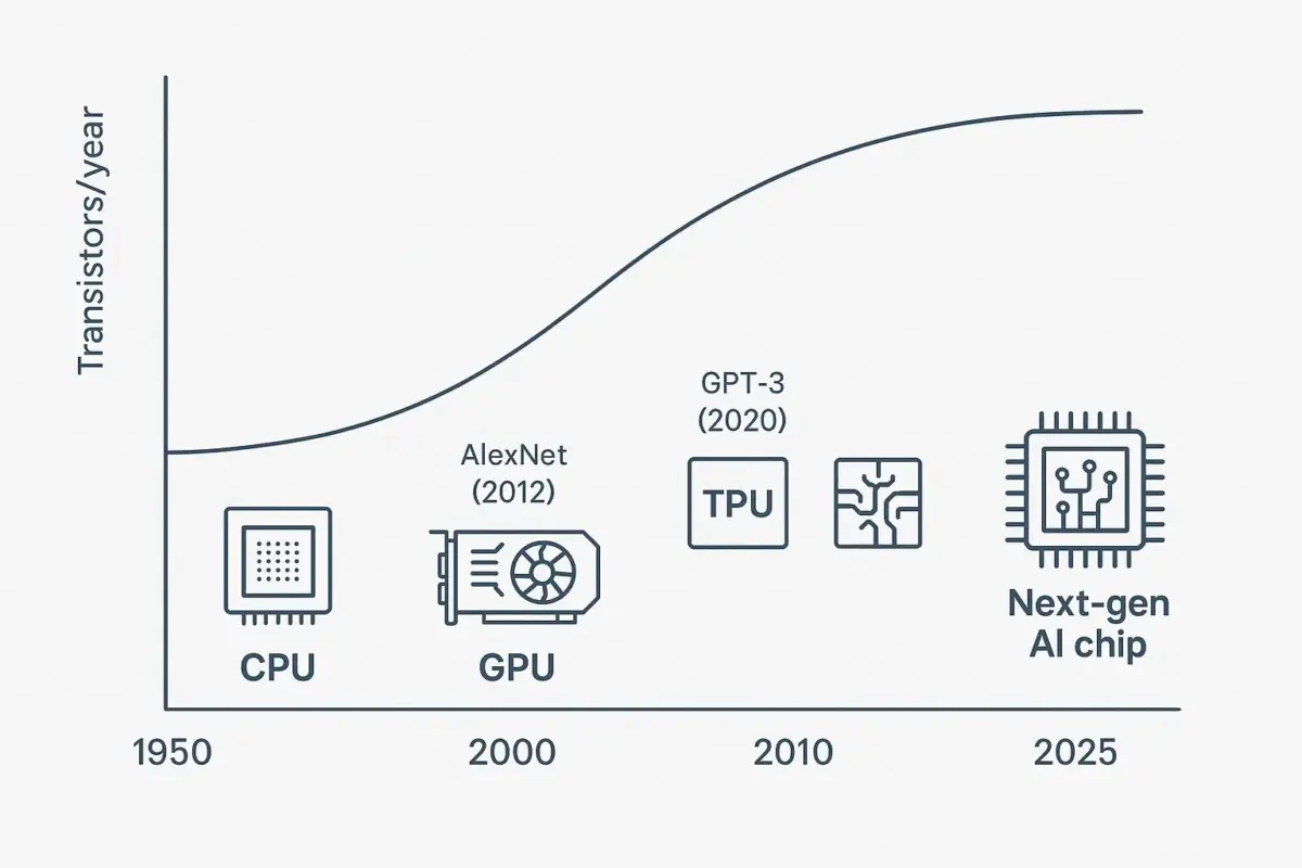
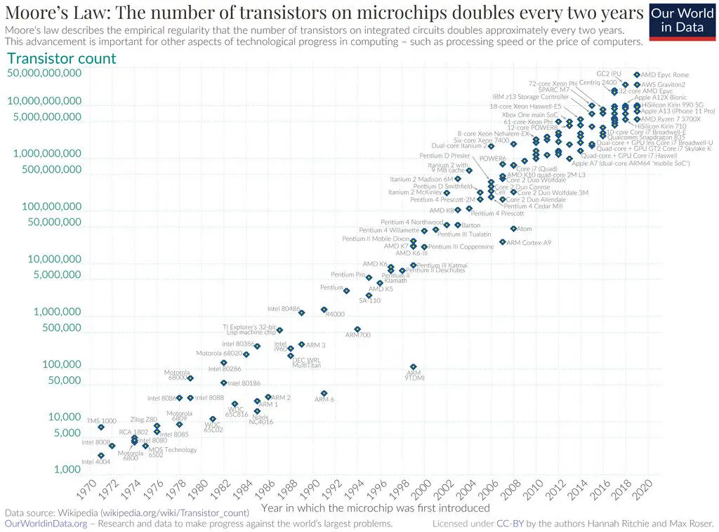
Moore’s Law states that the number of transistors will double every second year, roughly.This prediction has created a global need for highly advanced and highly miniaturized capacitors. Due to the enormous scaling of transistors in advanced processor chips, the need for decoupling capacitors mounted extremely close to the processor chip has exploded in recent years.
However, traditional capacitor technologies have difficulties delivering high enough performance in a small enough form factor.
Smoltek’s patent protected nanotechnology enables next-generation capacitors with extremely high electrical performance in a very small form factor.
Smoltek’s capacitors, called CNF-MIM (Carbon Nanofiber Metal-Insulator-Metal), can be placed directly adjacent to the circuits they are to support – the key to the rapidly growing market for decoupling capacitors for high-end processors – such as AI, High-Performance Computing and edge devices.
CNF-MIM capacitors meets the semiconductor industry’s demands for next-generation capacitors with unique characteristics:
* Capacitance is the ability of a component or circuit to collect and store energy in the form of an electrical charge.
Capacitors intended for use in next-generation AI chips and high-performance computing technology need to be able to handle the following:
Now, it’s fair to say that CNF-MIM is not the only technology for decoupling and energy storage in next-generation advanced chips. It’s competing with two other big capacitor technologies; Trench Silicon Capacitors, or Deep Trench Capacitors (TSC/DTC) and Multilayer Ceramic Capacitors (MLCC). The three technologies are all used for decoupling and energy storage, but they differ greatly in design, performance and integration.
Let’s take a look.
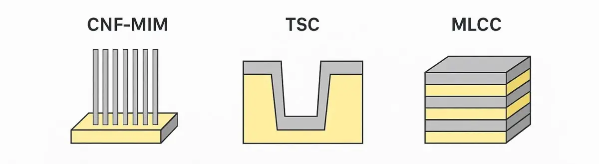
| Characteristic | CNF-MIM | TSC / DTC | MLCC |
| Placement | Directly under chip/interposer | In silicon/interposer | On PCB |
| Capacitance density | Very high (nanostructure) | High (trench structure) | Moderate (bulk) |
| ESR/ESL | Very low | Low | Relatively high |
| Integration | Future technology for AI/HPC | Already established in advanced packaging | Standard component, not chip-integrated |
| Maturity | In Development | Very mature and mass-produced | Very mature and mass-produced |
In conclusion, by pioneering carbon nanotechnology Smoltek has a truly disruptive capacitor technology that enables the combination of extremely high electrical performance in a highly miniaturized product. Smoltek Semi’s CNF-MIM capacitor addresses key challenges for next-generation AI, high-performance computing and edge devices.
Okay, so this has been a deep dive into the development of AI and what is required of the capacitors to keep this, not-so-new, thing rolling.
But the first question – what is AI wasn’t really answered, was it? That might take some time to explain though. Might as well ask the AI about it.
“Thanks for asking. AI, or Artificial Intelligence, refers to computer systems designed to perform tasks that typically require human intelligence, such as learning, problem-solving, decision-making, and language understanding. It uses algorithms to analyze data, identify patterns, and make decisions to achieve specific goals, with common examples including virtual assistants, recommendation systems, and self-driving cars.”
“High-performance computing (HPC) uses aggregated computing power, such as supercomputers or clusters of computers, to solve large, complex problems in science, engineering, and business that would be impossible on a typical computer. HPC systems process massive datasets and perform calculations at extremely high speeds, enabling complex modeling, data analysis, and artificial intelligence applications that drive innovation and provide significant competitive advantages.”
“Edge devices are hardware components, like routers, sensors, smartphones, and gateways, that connect to a core network and process data at or near its source, rather than sending it to a centralized cloud or data center for analysis. These devices are essential for edge computing, enabling real-time data processing, reducing latency, and improving network efficiency in applications ranging from the Internet of Things to industrial automation and smart cities.”
So, there you have it. An overview of AI developments and how Smoltek’s CNF-MIM capacitor technology has the potential to become an important pillar of energy-efficient power management in future chips.
Want to learn more about the extremely small and ultra-thin CNF-MIM capacitor? Go here!
Your data will be handled in compliance with our privacy policy.
IR Blog Posts
January 9, 2025
Modern electronics demand increasingly compact and powerful capacitors, and the race for miniaturization has reached a critical juncture. While both Deep Trench Capacitors (DTC) and Carbon Nanofiber Metal-Insulator-Metal (CNF-MIM) capacitors are being developed for advanced applications requiring smaller size and higher capacitance density than conventional surface-mounted capacitors, DTC pushes the boundaries of what’s achievable with subtractive manufacturing, but is hitting fundamental physical limits. In contrast, Smoltek’s innovative CNF-MIM technology offers a revolutionary path forward, unrestricted by these constraints.
IR Blog Posts

October 1, 2024
Smoltek Semi has developed a new material for use in CNF-MIM capacitors. The new material increases capacitance by more than three times and reduces leakage current by 50 percent. In this article, we examine what this means and why it is good for shareholders and investors.
IR Blog Posts
October 11, 2024
Our innovative “zapping” method drastically reduces development time and costs, enabling us to advance CNF-MIM technology faster and making Smoltek Semi’s technology even more attractive to potential buyers. Read on to see how this new process strengthens our position and shortens our path to market.
IR Blog Posts

June 16, 2025
Smoltek Semi joins an elite club of companies achieving 1 µF/mm² capacitance density, but stands alone in reaching this milestone with an ultra-thin profile. This breakthrough unlocks the under-chip real estate that represents the holy grail of capacitor placement in modern electronics.
IR Blog Posts

July 30, 2025
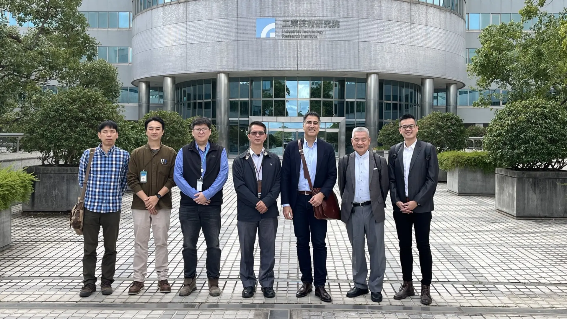
The recently signed technical service agreement between Smoltek Semi and the Industrial Technology Research Institute (ITRI) of Taiwan changes how CNF-MIM capacitors will reach the market. This partnership delivers the validation and manufacturing capabilities needed to transform laboratory breakthroughs into commercial reality.
News
June 18, 2025
Smoltek Semi has initiated the signing of a technical service agreement with the Taiwanese Industrial Technology Research Institute (ITRI) that enables low-volume production of Smoltek's propriety CNF-MIM capacitors.