Sign up for our newsletter!
Your data will be handled in compliance with our privacy policy.

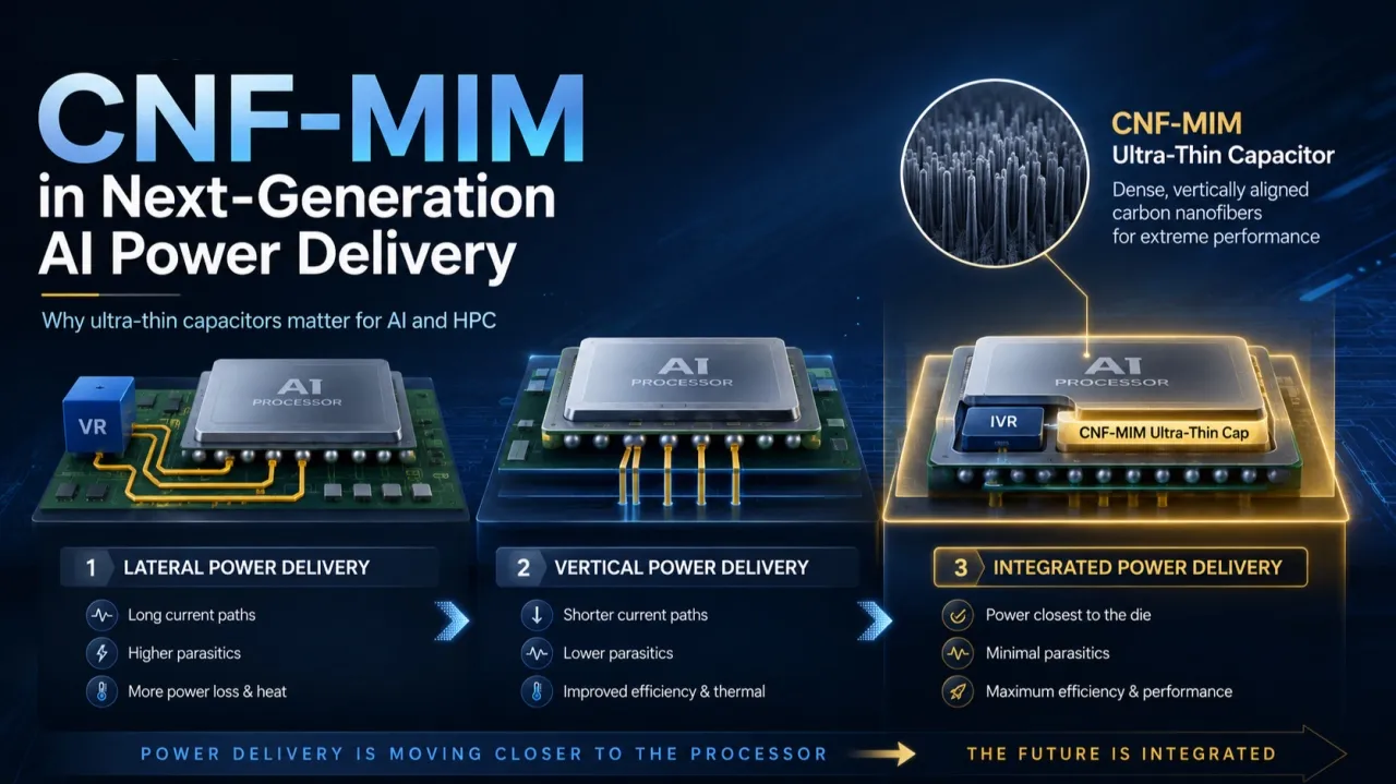
For many years, the performance story in AI and high-performance computing (HPC) was dominated by transistors and memory bandwidth. But as AI accelerators move into the kilowatt era, another limitation is becoming just as important: power delivery.
F A Ghavanini • June 29, 2026
Modern AI processors do not only need more power. They need power delivered at very high current and with extremely fast transient response. That combination creates a brutal engineering problem. At a core rail below 1 V, a 700 W accelerator corresponds to hundreds of amps of current. If we assume a 0.8 V rail, the current is approximately 875 A.
At that level, tiny parasitics are no longer tiny. A resistance of only 0.1 mΩ creates an 87.5 mV voltage drop. A loop inductance of only 10 pH exposed to a 10 A/ns current transient creates a 100 mV voltage disturbance. These numbers are large compared with the available voltage margin on a sub‑1 V rail.
This is why power delivery has become one of the defining challenges in AI and HPC hardware, with capacitors playing a central role in determining system performance, efficiency, and reliability.
The first generation of high-power accelerator boards largely followed the same logic used in servers and graphics cards for many years. Voltage regulators, inductors and capacitors were placed around the processor or accelerator package. Power was converted on the board and then routed laterally across the PCB and package to reach the silicon.
This approach is practical and familiar. It uses mature multiphase voltage-regulator modules, proven PCB manufacturing and a large ecosystem of discrete multilayer ceramic capacitors (MLCCs) and inductors. Looking at AI accelerator boards such as the NVIDIA H100 generation, the basic architecture is still recognizable: high-power inputs, board-level conversion and dense clusters of power components around the main package.
For the H100 SXM form factor, NVIDIA specifies a thermal design power of up to 700 W. The PCIe version is lower power, but still represents a very high-current power-delivery challenge. The important point is not only the absolute power. It is the fact that this power must ultimately be delivered to low-voltage rails close to the die.
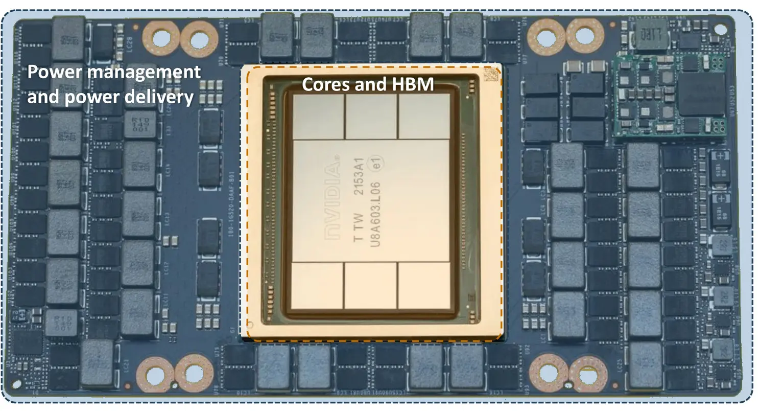
Lateral power delivery works, but it scales poorly as current rises. A capacitor can only support fast transients effectively if the path between the capacitor and the load has very low resistance and impedance. When the capacitor is placed too far away, as is the case in lateral power delivery, the added resistance and inductance slow down its response and reduce its ability to deliver charge exactly when the processor needs it. The result is higher voltage droop, more supply noise, reduced power efficiency and a growing need for capacitors that can be placed much closer to the die.
This is the first major opening for ultra-thin capacitors. Thanks to their very low-profile form factor, they enable decoupling to move much closer to the point of load — something that is not realistically possible with conventional MLCC banks.
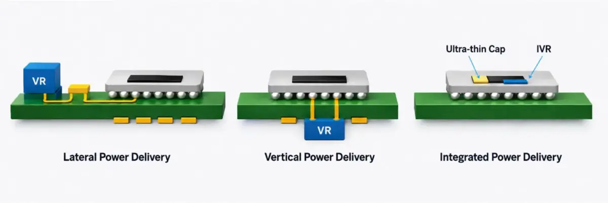
Instead of routing high current sideways across the board, compact power modules can be placed underneath the processor and push power vertically upward through the board and package. This shortens the high-current path, reduces conduction loss and improves power integrity. This is a major improvement for AI and HPC processors because it attacks the two key problems at once: resistance and inductance.
To preserve the benefit of this architecture, decoupling capacitors must also move closer to the point of load, often into spaces where conventional capacitor banks cannot fit. This requires capacitors that are not only extremely thin, but also capable of delivering low ESR, low ESL and high capacitance density in a very small volume. That combination makes ultra-thin capacitors a key enabling technology for vertical power delivery.
However, traditional capacitor technologies have difficulties delivering high enough performance in a small enough form factor.
At its most fundamental level, a capacitor is a simple device: two conductive electrodes separated by an insulating dielectric. The more electrode surface area that can be packed into a given volume, the more capacitance can be achieved in that same footprint.
This is why the geometry of the electrode structure matters so much. For conventional planar capacitors, the available surface area is limited by the footprint of the device. To increase capacitance density, the industry has therefore moved toward three-dimensional structures that increase the effective electrode area without increasing the footprint of the component.
There are two main ways to do this:
This is the principle behind Smoltek’s proprietary carbon nanofiber-based metal-insulator-metal (CNF-MIM) technology. Smoltek grows vertically aligned carbon nanofibers from the surface, creating a dense forest of conductive nanostructures with extremely high aspect ratio. These carbon nanofibers dramatically increase the available electrode surface area within a very small volume. A conformal dielectric layer is then deposited around the nanofibers, followed by the top electrode, forming a metal-insulator-metal capacitor in a three-dimensional nanostructured geometry.
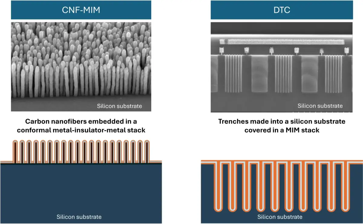
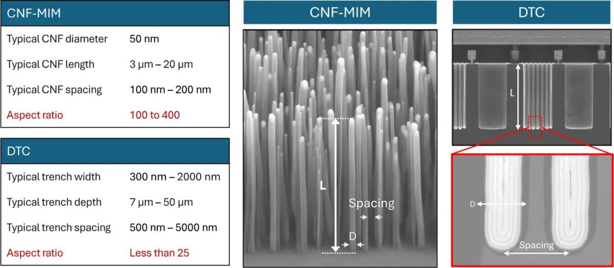
One key difference between CNF-MIM and deep trench capacitors is the aspect ratio of the underlying 3D structure that creates the capacitor surface area. In DTC technology, the surface gain comes from trenches etched into silicon resulting in aspect ratios typically below 25. In Smoltek’s CNF-MIM technology, the 3D structure is instead formed by vertically aligned carbon nanofibers with an average diameter of less than 100 nm resulting aspect ratios of exceeding 100 (see Figure 4). This much higher aspect ratio means that CNF-MIM can generate significantly more electrode surface area in the same volume.
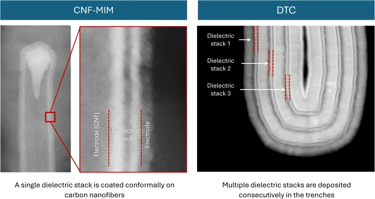
The higher aspect ratio of CNF-MIM also translates directly into a cost advantage. Because deep trench capacitors have a lower aspect ratio, they often need to compensate by depositing multiple metal-insulator-metal stacks inside the trenches to reach high capacitance density. Each additional electrode and dielectric layer adds process complexity and increases the fabrication cost, especially because these films are typically deposited using low-throughput ALD processes. CNF-MIM, by contrast, can achieve high capacitance density with a single dielectric stack coated conformally over the carbon nanofibers.
In addition, DTC requires high-resolution lithography to define dense and narrow trench structures, while CNF-MIM nanofibers can be grown from catalyst nanoparticles formed by dewetting of a continuous catalyst film. This eliminates the need for costly high-resolution lithography and gives CNF-MIM a simpler and cheaper route to high capacitance density.
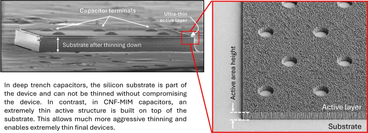
Another important advantage of CNF-MIM is that it is substrate agnostic. In deep trench capacitors, the silicon substrate is an integral part of the device because the capacitor surface area is created by etching trenches into the silicon. This makes the technology inherently tied to silicon and limits its transferability to other substrate platforms. In contrast carbon nanofibers are grown on top of the substrate.
In fact, Smoltek has already demonstrated CNF growth on a variety of materials, including silicon, glass, alumina, stainless steel foil, copper foil and aluminum foil. This flexibility is strategically important because future power-delivery architectures will not be limited to silicon alone.
For example, glass substrates are gaining interest for advanced interposers because of their dimensional stability, fine-line routing potential and suitability for large-area panel-level integration.
A capacitor technology that can be implemented on glass offers a broader integration path for advanced packaging, embedded capacitance and vertical power-delivery solutions.
The next step is to move the voltage regulation even closer to the point of load.
Integrated voltage regulators and compact power-converter chiplets are part of this trend. Instead of placing the regulator only on the board, future architectures may place power conversion on the land side of the package, inside the package substrate, or close to the die itself. The objective is clear: reduce the distance between the regulator, the decoupling capacitor and the load.
This is a logical continuation of the same trend. Lateral power delivery placed power around the processor. Vertical power delivery moved power underneath the processor. Package-level and integrated power delivery bring conversion and decoupling even closer to the point of load. At that point, thickness becomes the critical differentiator. This is where CNF-MIM has a decisive advantage over DTC: it can be made thinner.
In deep trench capacitors, the silicon substrate is not just a carrier; it is part of the capacitor itself because the trenches are etched into it. This limits how aggressively the wafer can be thinned without compromising the device. CNF-MIM is fundamentally different. The ultra-thin active capacitor structure is built additively on top of the substrate, while the substrate mainly serves as a carrier. This allows much more aggressive thinning and enables final devices as thin as 40 µm, compared with roughly 100 µm for typical DTC solutions.
Moreover, the ultra-thin active capacitor layer can be formed directly on substrates that are already very thin, such as metal foils or other flexible carrier materials. Instead of relying on a thick silicon wafer that must later be etched and thinned, CNF-MIM can in principle be built where the final form factor is defined primarily by the starting substrate and the few-micrometer-thick active layer.
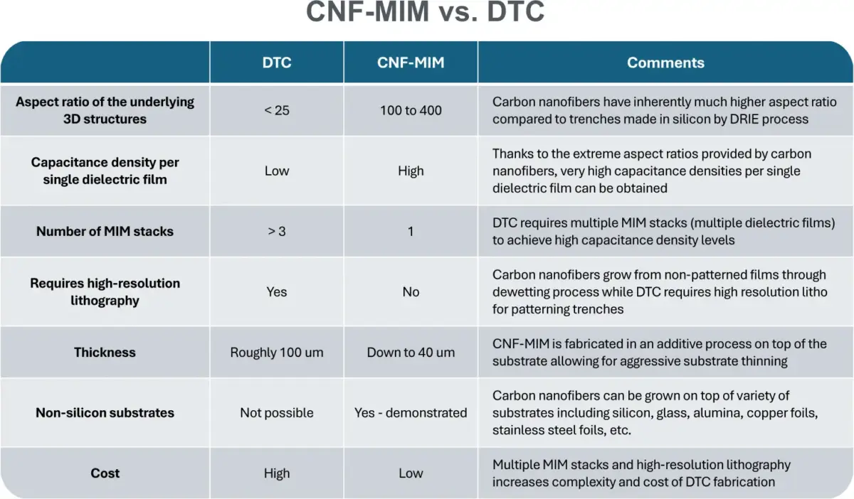
First, CNF-MIM offers a more attractive path to cost-efficient high capacitance density. Deep trench capacitors create surface area by etching narrow structures into silicon, which requires demanding lithography and deep silicon processing. Because the trench aspect ratio is limited, DTC technology often needs multiple metal-insulator-metal stacks to compensate and reach high capacitance density. That adds process complexity, ALD time and cost. CNF-MIM takes a different route. It creates high surface area additively, by growing carbon nanofibers from the surface, and can achieve high capacitance density with a single conformal dielectric stack. This makes CNF-MIM not only technically different, but potentially simpler and cheaper to manufacture.
Second, CNF-MIM is not locked to silicon. This is strategically important. Since the active nanofiber structure is grown on top of the substrate, the same basic concept can be transferred to different carrier materials, including glass, alumina, stainless steel, copper and aluminum. Glass is especially important for the future of advanced packaging and scalable integration, where large-area processing, dimensional stability and fine-line routing are becoming increasingly attractive. A capacitor technology that can move beyond silicon and follow the industry toward new package and interposer platforms has a much stronger long-term integration path.
But the most important advantage is thickness. Future power delivery is moving from the board to underneath the processor, to the package, and eventually as close as possible to the silicon itself. In that world, every micrometer matters. A capacitor is no longer useful only because it has high capacitance density; it must also fit into extremely limited vertical space. This is where CNF-MIM wins most clearly. In DTC, the silicon substrate is part of the capacitor structure itself, because the trenches are etched into it. That limits how far the device can be thinned. In CNF-MIM, the active capacitor is built additively on top of the substrate, while the substrate mainly acts as a carrier. This makes much more aggressive thinning possible and enables devices down to around 40 µm.
This combination is what makes CNF-MIM such a strong candidate for the next generation of ultra-thin decoupling capacitors. It offers a potentially lower-cost route to high capacitance density, it can be integrated into future-relevant substrates such as glass, and above all, it can be made extremely thin. As power delivery moves closer to the processor, that thickness advantage becomes decisive.
Learn more about the extremely small and ultra-thin CNF-MIM capacitor: Go here!
Your data will be handled in compliance with our privacy policy.
IR Blog Posts

January 9, 2025
Modern electronics demand increasingly compact and powerful capacitors, and the race for miniaturization has reached a critical juncture. While both Deep Trench Capacitors (DTC) and Carbon Nanofiber Metal-Insulator-Metal (CNF-MIM) capacitors are being developed for advanced applications requiring smaller size and higher capacitance density than conventional surface-mounted capacitors, DTC pushes the boundaries of what’s achievable with subtractive manufacturing, but is hitting fundamental physical limits. In contrast, Smoltek’s innovative CNF-MIM technology offers a revolutionary path forward, unrestricted by these constraints.
IR Blog Posts

October 1, 2024
Smoltek Semi has developed a new material for use in CNF-MIM capacitors. The new material increases capacitance by more than three times and reduces leakage current by 50 percent. In this article, we examine what this means and why it is good for shareholders and investors.
IR Blog Posts

October 11, 2024
Our innovative “zapping” method drastically reduces development time and costs, enabling us to advance CNF-MIM technology faster and making Smoltek Semi’s technology even more attractive to potential buyers. Read on to see how this new process strengthens our position and shortens our path to market.
IR Blog Posts

June 16, 2025
Smoltek Semi joins an elite club of companies achieving 1 µF/mm² capacitance density, but stands alone in reaching this milestone with an ultra-thin profile. This breakthrough unlocks the under-chip real estate that represents the holy grail of capacitor placement in modern electronics.
IR Blog Posts

July 30, 2025
The recently signed technical service agreement between Smoltek Semi and the Industrial Technology Research Institute (ITRI) of Taiwan changes how CNF-MIM capacitors will reach the market. This partnership delivers the validation and manufacturing capabilities needed to transform laboratory breakthroughs into commercial reality.
News
June 18, 2025
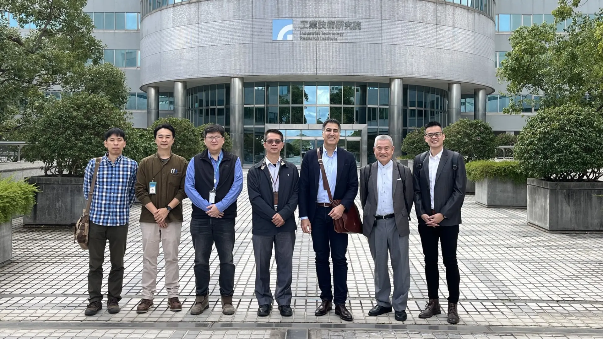
Smoltek Semi has initiated the signing of a technical service agreement with the Taiwanese Industrial Technology Research Institute (ITRI) that enables low-volume production of Smoltek's propriety CNF-MIM capacitors.