Sign up for our newsletter!
Your data will be handled in compliance with our privacy policy.

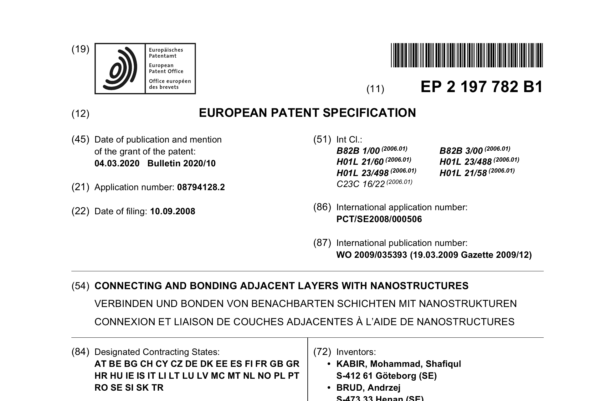
The Bumping family is an apparatus connecting and bonding adjacent layers with nanostructures.
J Berg, V Desmaris, S Kabir, A Brud • September 10, 2008
The invention: An apparatus comprising two conductive surfaces or layers and a nanostructure assembly bonded to the two conductive surfaces or layers to create electrical or thermal connections between the two conductive surfaces or layers, and a method of making same.
| Patent Office | Patent |
|---|---|
| China | CN101827782 |
| China | CN104600057 |
| Europe | EP2197782 |
| Japan | JP5535915 |
| Japan | JP6149077 |
| South Korea | KR101487346 |
| Taiwan | TWI511208 |
| Taiwan | TWI564980 |
| Taiwan | TWI655695 |
| USA | US8106517 |
| USA | US8253253 |
| USA | US8815332 |
Your data will be handled in compliance with our privacy policy.