Sign up for our newsletter!
Your data will be handled in compliance with our privacy policy.

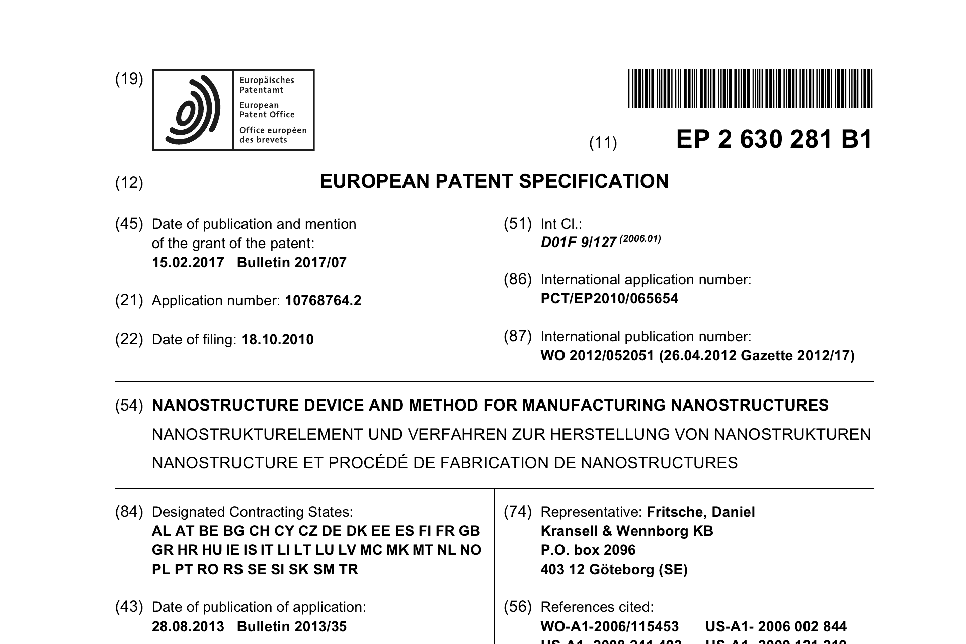
The Catalyst Diffusion family is covering a method for manufacturing a plurality of nanostructures on a substrate.
A M Saleem, D Brud, J Berg, S Kabir, V Desmaris • October 18, 2010
The invention: Nanostructure device and method for manufacturing nanostructures – A method for manufacturing a plurality of nanostructures on a substrate. The method comprises the steps of: depositing a bottom layer on an upper surface of the substrate, the bottom layer comprising grains having a first average grain size; depositing a catalyst layer on an upper surface of the bottom layer, the catalyst layer comprising grains having a second average grain size different from the first average grain size, thereby forming a stack of layers comprising the bottom layer and the catalyst layer; heating the stack of layers to a temperature where nanostructures can form; and providing a gas comprising a reactant such that the reactant comes into contact with the catalyst layer.
| Patent Office | Patent |
|---|---|
| China | CN103154340 |
| Europe | EP2630281 |
| India | IN347659 |
| Russia | RU2573474 |
| South Korea | KR101736303 |
| South Korea | KR101903714 |
| South Korea | KR101970209 |
| USA | US9206532 |
Your data will be handled in compliance with our privacy policy.