Sign up for our newsletter!
Your data will be handled in compliance with our privacy policy.
Your data will be handled in compliance with our privacy policy.

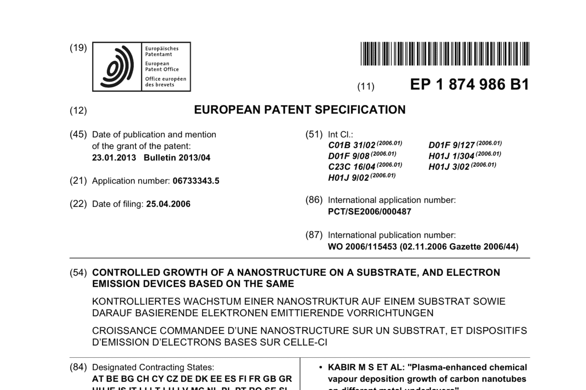
The Interconnects A family is covering a method regarding controlled growth of a nanostructure on a substrate, and electron emission devices based on the same.
A method of forming of nanostructures and nanostructure devices — A truly unique nanostructure growth platform technology that enables manufacturing of nanomaterial devices on CMOS platform. The method covers different types of nanostructures including carbon nanotubes, nanofibers, nanowires, etc.
The present invention provides a method for nanostructures grown on a metal underlayer, and a method of making the same. The grown nanostructures based on the claimed method are suitable for manufacturing electronic devices such as an electron beam writer, and a field emission display.
Your data will be handled in compliance with our privacy policy.
Oops! Someone forgot to publish content. We apologize for the inconvenience.