Sign up for our newsletter!
Your data will be handled in compliance with our privacy policy.
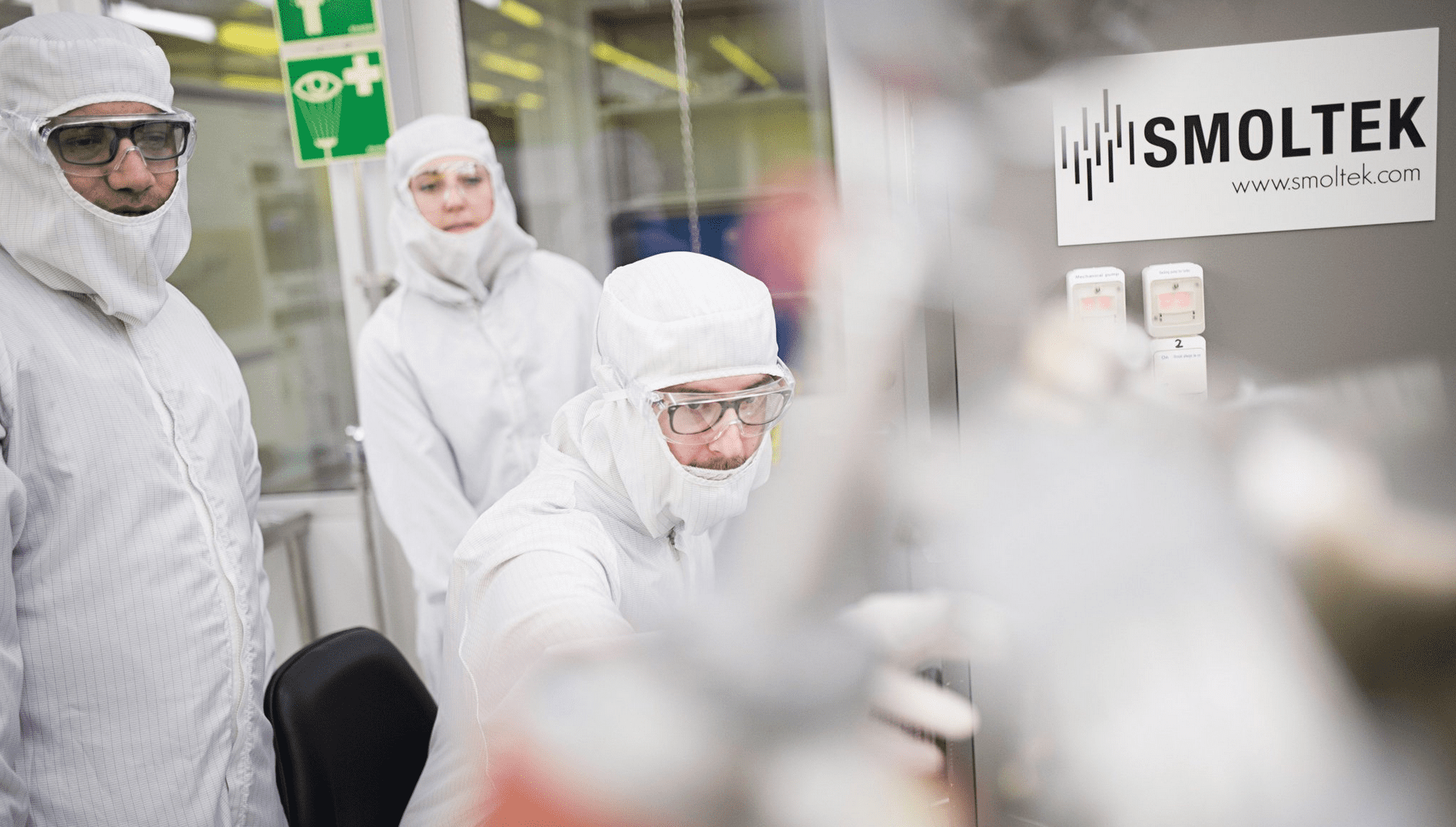
Are you an experienced and hands-on Semiconductor R&D Manager – ALD? Apply today!
Smoltek Semi AB is pioneering ultra-thin carbon nanofiber-based metal-insulator-metal (CNF-MIM) capacitor technology. To accelerate our technology platform towards manufacturable, high-performance products, we are looking for a technically strong and product-oriented Semiconductor R&D Project Manager to lead and coordinate our atomic layer deposition (ALD) activities.
You will drive ALD development using both Smoltek’s in-house ALD capability and external tools and development partners. The role combines technical depth with hands-on project leadership: translating product and device requirements into development plans, coordinating experiments and resources, and driving ALD processes from material development towards robust device integration and scalable manufacturing.
You will work closely with internal engineers as well as external laboratories, research institutes, equipment suppliers, and manufacturing partners, and will directly report to the CTO.
What you bring:
Smoltek is working on a technology you won’t find just anywhere; we combine carbon nanofibers with advanced thin films to enable next-generation capacitors. In this role, you will influence both the technical direction and the way our ALD development is executed, from materials and processes all the way to product-relevant solutions. The team is small, skilled, and collaborative, so decisions are close to the technology and good ideas can move quickly.
Send your application to recruitment@smoltek.com no later than October 24, 2026. Applications will be reviewed continuously.
Your data will be handled in compliance with our privacy policy.
News
October 24, 2025
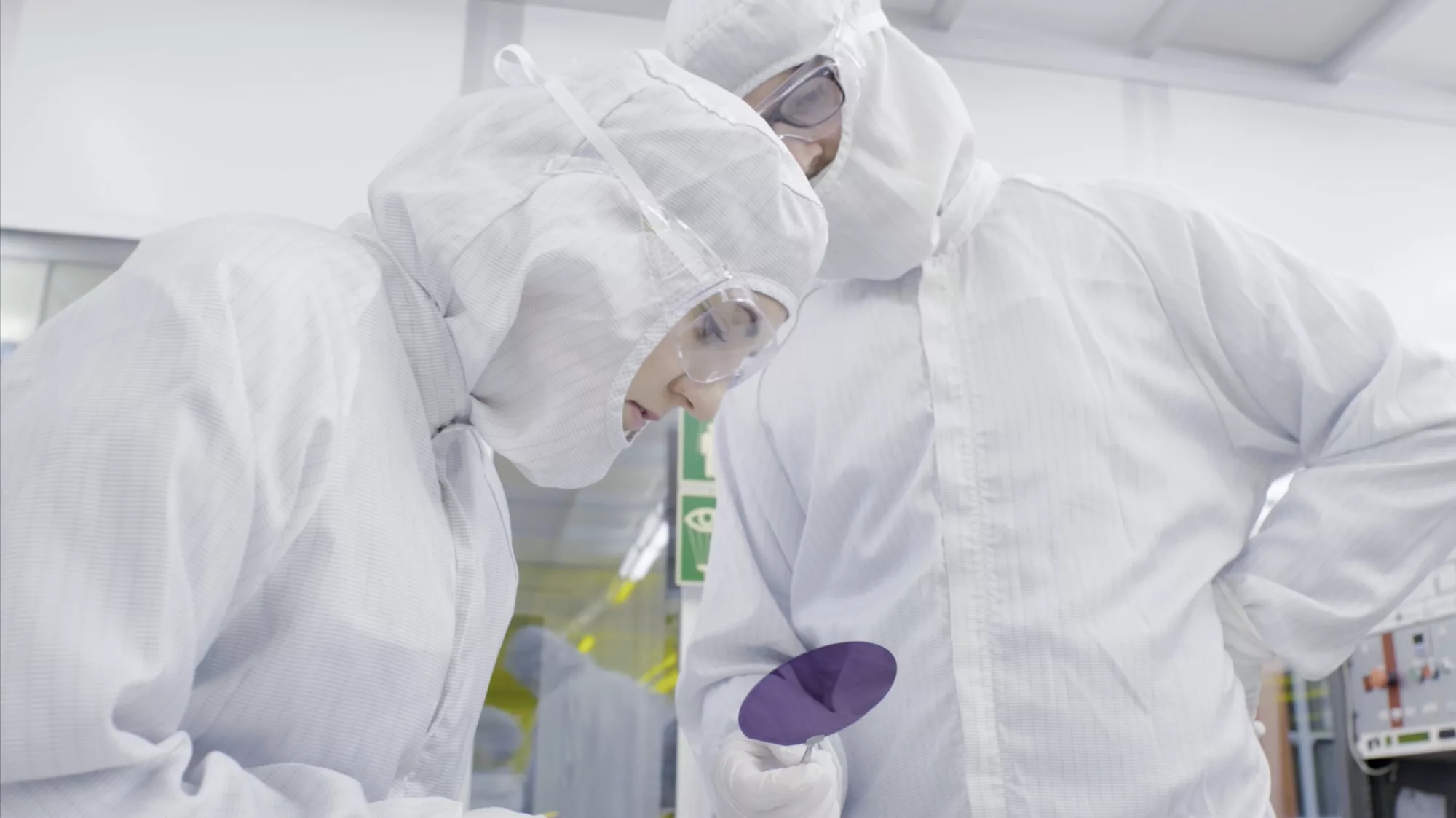
Smoltek Semi has acquired a plasma-enhanced Atomic Layer Deposition (ALD) system to implement its advanced dielectric stack on carbon nanofibers. The system will significantly reduce the iteration time of coating processes while enabling innovation and IP generation in dielectric stack technology for carbon nanofiber electrodes.
IR Blog Posts

June 16, 2025
Smoltek Semi joins an elite club of companies achieving 1 µF/mm² capacitance density, but stands alone in reaching this milestone with an ultra-thin profile. This breakthrough unlocks the under-chip real estate that represents the holy grail of capacitor placement in modern electronics.
News
June 11, 2025
Smoltek Semi has successfully engineered an advanced dielectric stack that surpasses 1 microfarad per Square millimeter capacitance milestone.
IR Blog Posts

July 30, 2025
The recently signed technical service agreement between Smoltek Semi and the Industrial Technology Research Institute (ITRI) of Taiwan changes how CNF-MIM capacitors will reach the market. This partnership delivers the validation and manufacturing capabilities needed to transform laboratory breakthroughs into commercial reality.
News
December 17, 2024
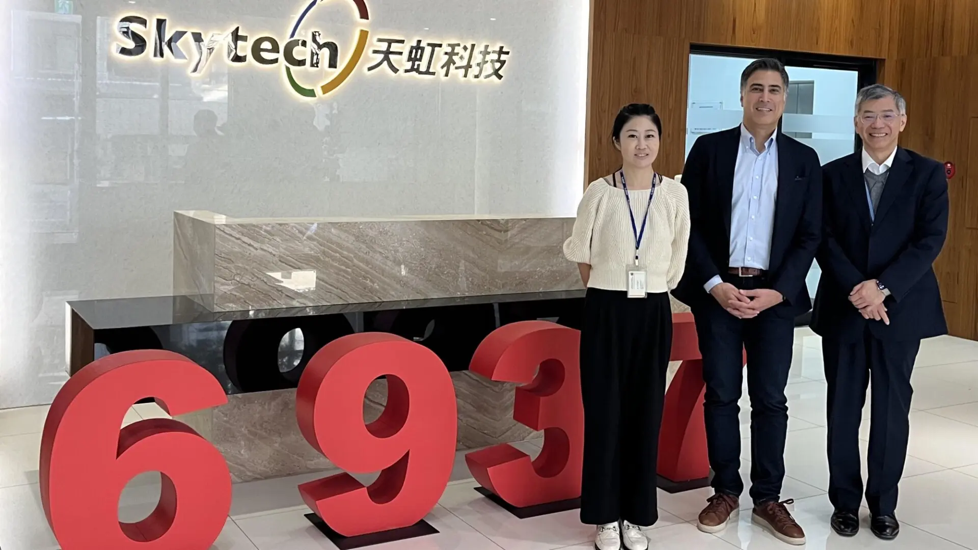
Dr. Farzan Ghavanini, CTO of Smoltek has been on a week-long business trip to Taiwan to visit some of our collaboration partners for CNF-MIM capacitors, among those ALD-company Skytech.
News
March 24, 2025
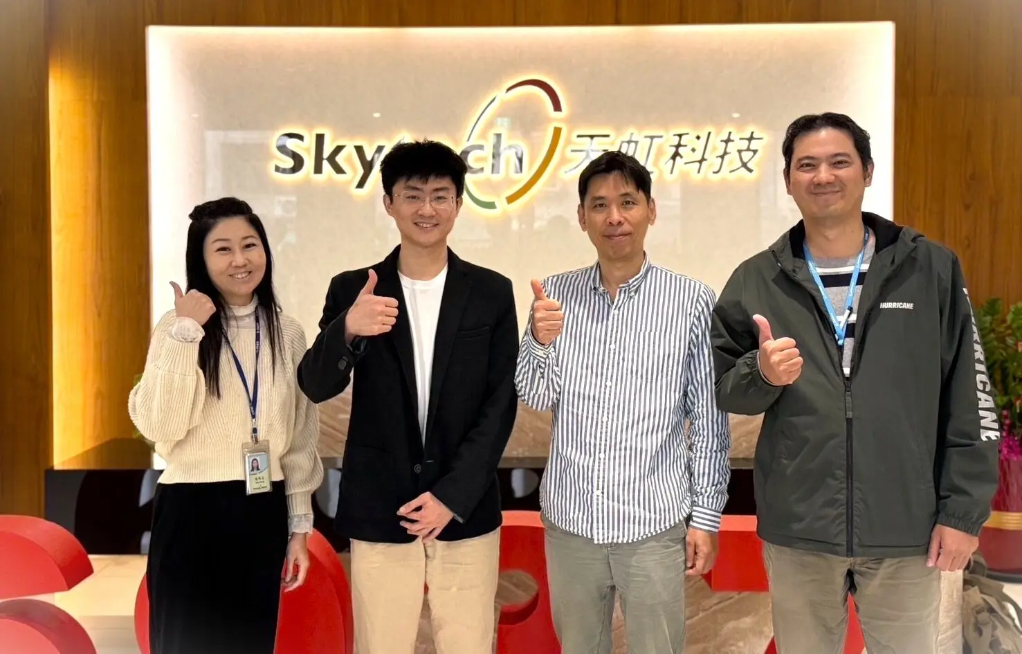
Qi Li and ChinJung Kuo of Smoltek Semi have met with Skytech management in Taiwan for planning of testing dummy runs for ALD deposition of Smoltek's CNF-MIM capacitors.