Sign up for our newsletter!
Your data will be handled in compliance with our privacy policy.
Your data will be handled in compliance with our privacy policy.


Yet another patent granted in Japan.
The new Japanese patent covers an aspect of how nanostructures can be exploited to be used for joining two adjacent layers or substrates for interconnecting purposes.This includes carbon nanotubes, nanofibers, nanowires etc.
“We are very happy to see our IP footprint is constantly increasing in Japan for both core growth and application related patents portfolio based on nanostructures,” says Dr. M. Shafiq Kabir, Smoltek´s CIO.
Smoltek’s patent portfolio now globally comprises 48 granted patents.
Read more about our patent portfolio here
Your data will be handled in compliance with our privacy policy.
News
August 8, 2024
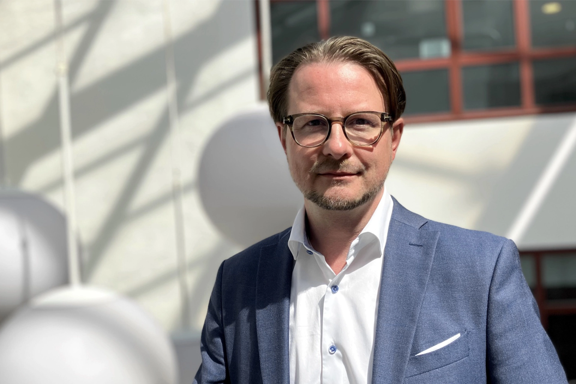
Smoltek’s board of directors has a new member: David Gramnaes. He is the CEO of Gramtec Venture, an investment company within the Gramtec group – one of Smoltek’s longest-standing investors and largest shareholder. In this interview, you get to know him and gain insight into how his experiences have shaped him and how this influences his work on the Board. He also talks candidly about Smoltek’s history and future and the turmoil surrounding Yageo.
News
August 13, 2021
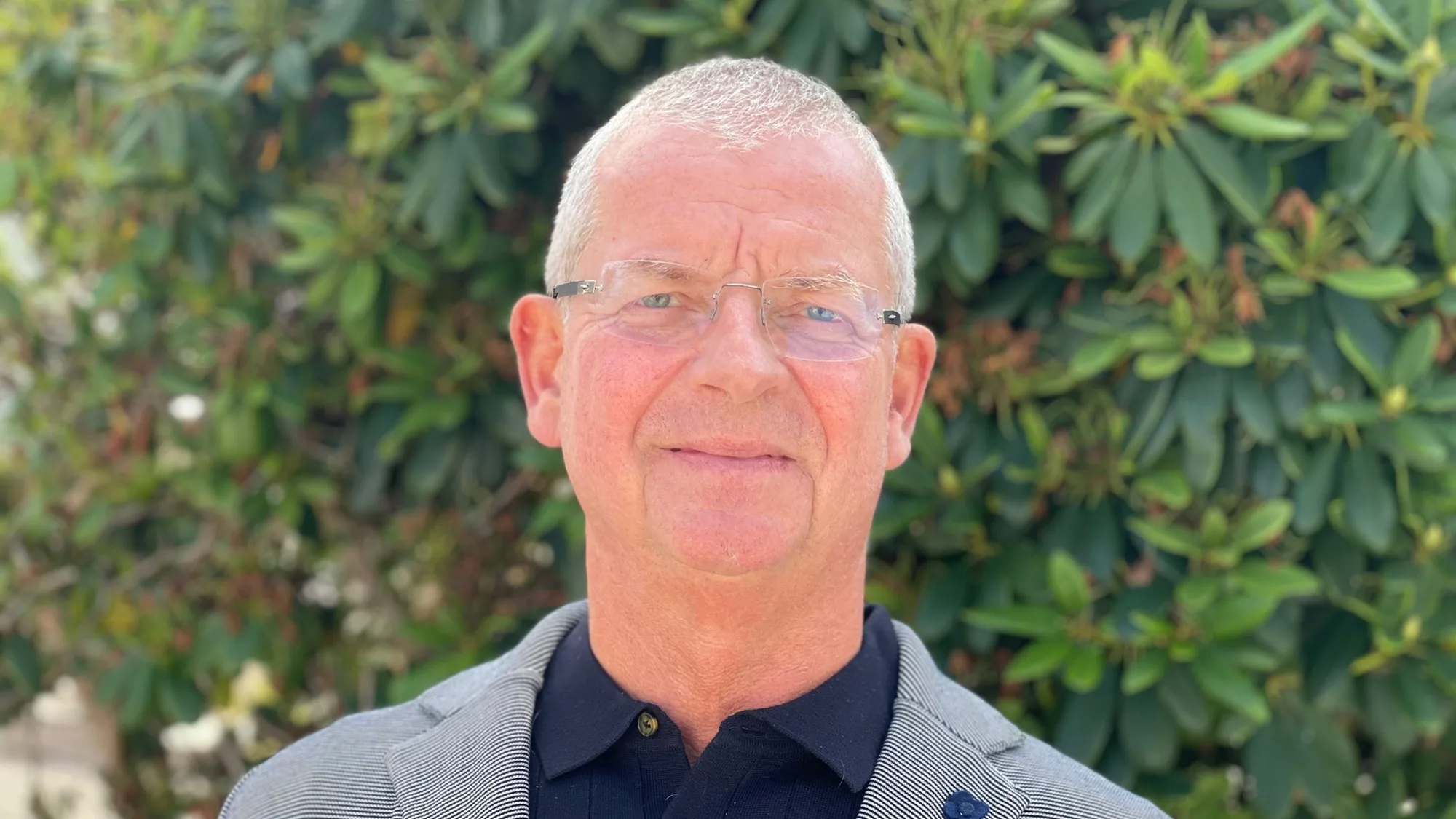
Håkan Persson, with many years of experience from leading and developing listed technology companies, will take over as CEO of Smoltek. He will join the company no later than October 15, maybe sooner. In anticipation of his accession, we have had a short Q&A with him.
News

August 18, 2020
Research Engineer Qi Li is a new member of the R&D-team at Smoltek. Qi will be working with the design, manufacturing and characterization of carbon nanostructure-based components.
News

December 6, 2019
Pia Tegborg will take over as new CFO for Smoltek, starting on January 1, 2020. The role also includes the responsibility for the company's IR communication.
News
November 21, 2019
Smoltek will be part of a Swedish business delegation going to Seoul, South Korea in December. This gives us the opportunity to connect and have a sit down with Korean semiconductor giants.
News
November 11, 2019
Ta chansen att träffa Smoltek på Stora Aktiedagen i Stockholm, måndag 25 november. VD Anders Johansson finns på plats på investerarmässan under dagen.