Sign up for our newsletter!
Your data will be handled in compliance with our privacy policy.
Your data will be handled in compliance with our privacy policy.

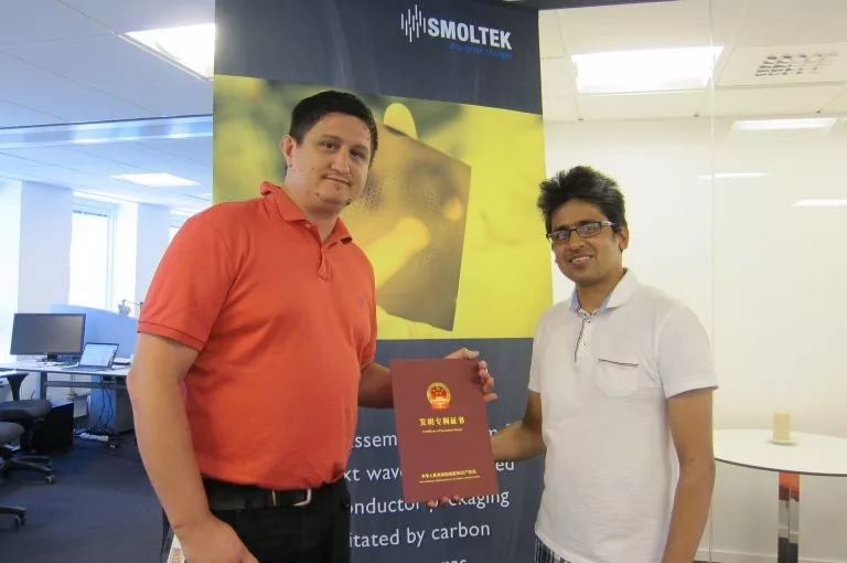
Smoltek has yet another granted patent to add to its extensive IP portfolio. This patent, the 49th of the company’s granted patents, is regulating patent rights on nanostructure processing in China.
The new Chinese patent strengthens the position of our helplayer patent family towards forming of nanostructure devices. The method covers different types of nanostructures including carbon nanotubes, nanofibers, nanowires etc.
“Another confirmation of our unique nanostructure growth platform technology that enables manufacturing of nanomaterial devices on CMOS platform. We are humbled to see that our IP footprint is constantly strengthening in China, one of the main hubs for semiconductor manufacturing”, says Dr. M. Shafiq Kabir, Smoltek´s CIO.
Smoltek’s patent portfolio now globally comprises 49 granted patents.
Your data will be handled in compliance with our privacy policy.
News
May 15, 2026
Smoltek has been granted an additional patent within its Interposer patent family, further protecting the company’s CNF-MIM capacitor technology for advanced semiconductor packaging. With this European patent approval, the company has secured Interposer IP in all major global markets.
News
March 27, 2026
Our CNF-MIM technology has demonstrated stable electrical performance after 2,000 hours in an independent life test conducted by a global capacitor manufacturer. This further strengthens confidence in the reliability of the technology and supports Smoltek's development of advanced capacitors for AI, RF and optoelectronics, among other applications.
News
February 24, 2026
An independent, third-party reliability test of our CNF-MIM capacitor technology has confirmed the reliability results communicated on February 5, 2026. The independent validation, performed by a major capacitor manufacturer, also reduces technical risk in the commercialization process and strengthens Smoltek’s credibility in ongoing negotiations with industrial partners.
News

February 5, 2026
Smoltek’s CNF-MIM capacitors demonstrate excellent stability in a new 1,000-hour life test at 85°C under applied 2 volts. No degradations were observed, and the capacitors exhibited more than 1,000 times lower current leakage compared to the previous life test.
News

November 20, 2025
We have launched a podcast about materials technology and investments in general and our disruptive carbon nanotechnology in particular.
News
November 17, 2025
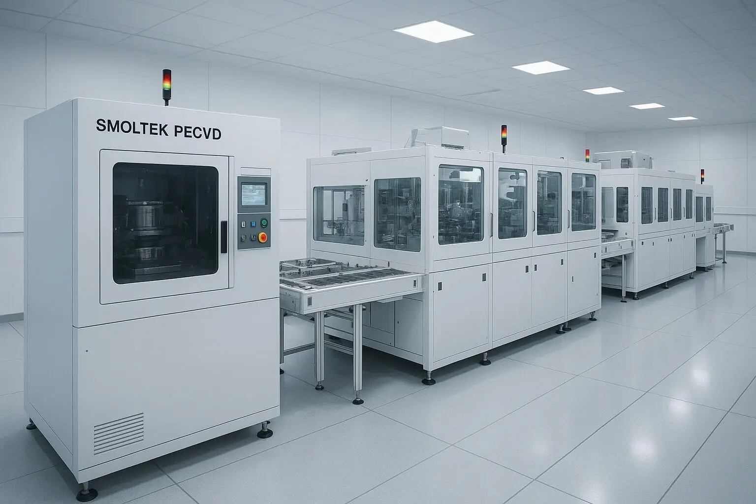
Smoltek Semi is currently optimizing the company’s advanced PECVD system to ensure implementation of its most recent technological innovations in CNF synthesis, enabling compliance with stringent customer requirements, prior to installation at ITRI in Taiwan.