Sign up for our newsletter!
Your data will be handled in compliance with our privacy policy.
Your data will be handled in compliance with our privacy policy.


Smoltek Semi has developed a process for manufacturing of engineering samples in high volumes. This process will now be tested for production of CNF-MIM engineering samples in high volumes, as the first trial-run of capacitor prototypes (without the patent protected carbon nanofibers) was successful.
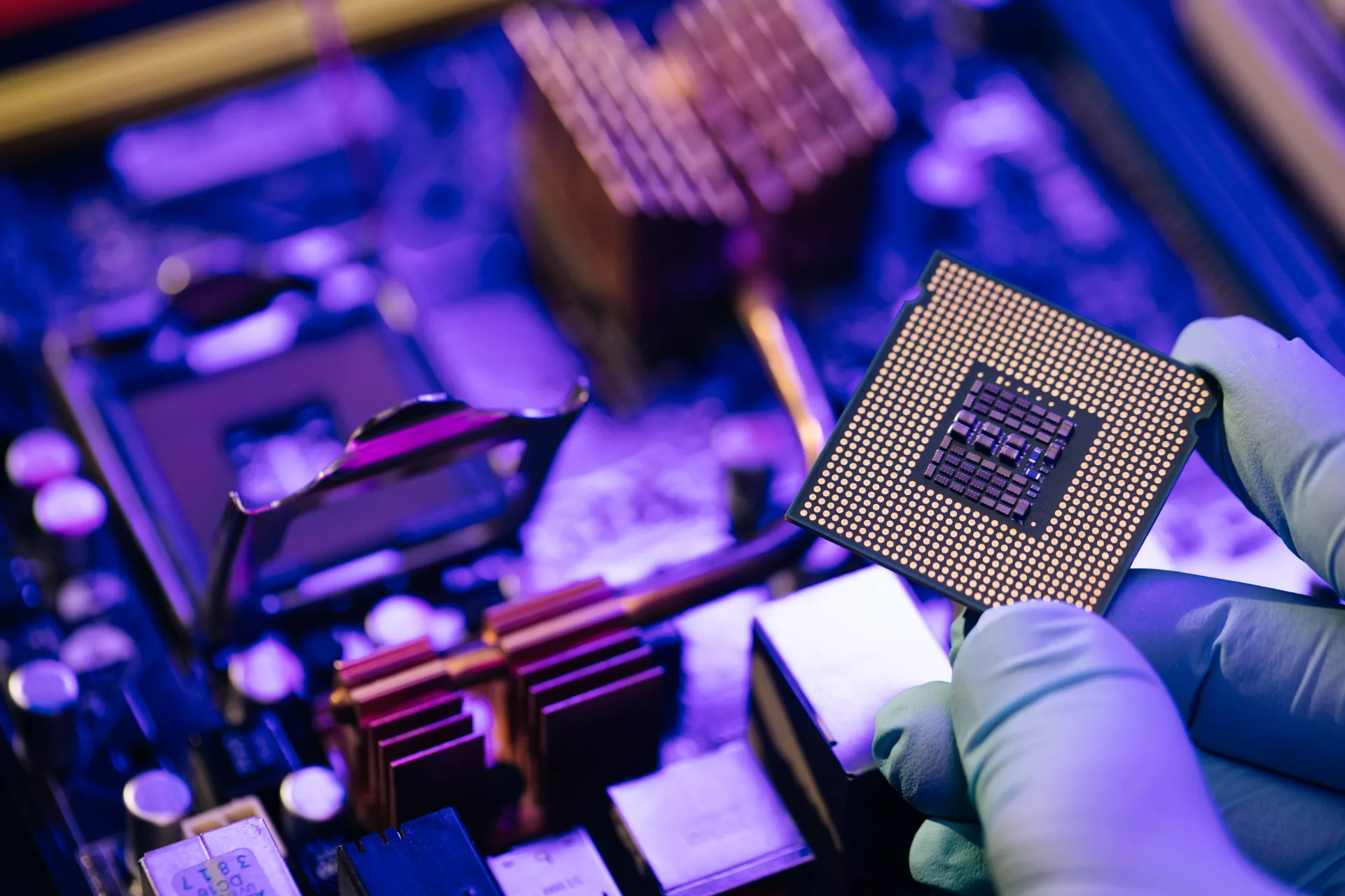
Smoltek Semi has successfully manufactured capacitor prototypes (without carbon nanofibers) on 8‑inch wafer format. The processing has been carried out in collaboration with several manufacturing partners, including research institutes, tool vendors as well as high-volume foundries. Most of the processing has been made on standard high-volume production tools used for component production in the semiconductor industry.
The capacitor prototypes have the purpose of developing and validating the stability, repeatability, and overall quality of the fabrication processes necessary for 8‑inch wafer format production – not to demonstrate high electrical performance of our CNF-MIM capacitors.
Louise Duker, Chief Product Officer at Smoltek Semi.
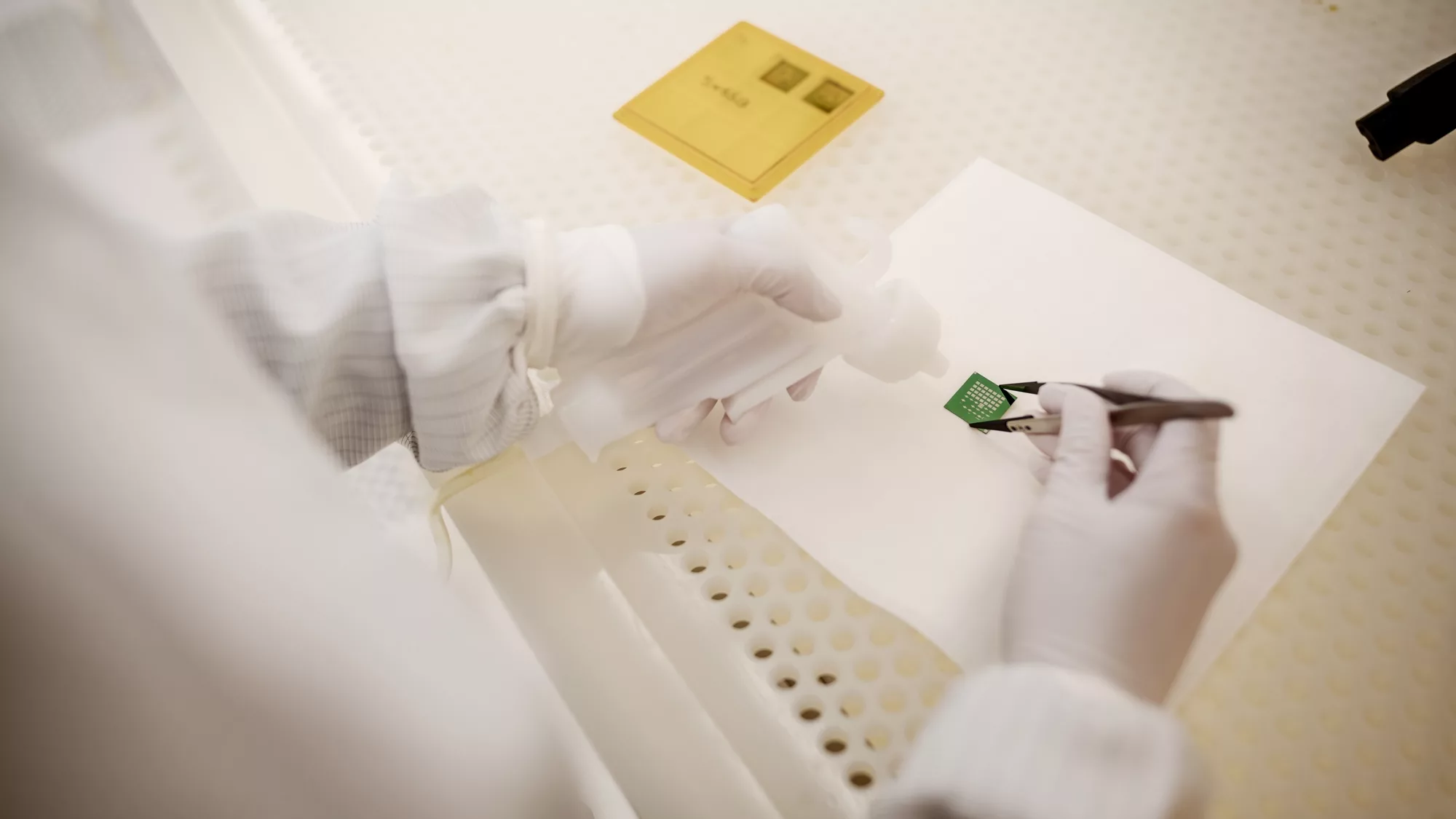
Based on the successful results achieved, Smoltek Semi has decided to utilize the developed 8‑inch fabrication process to produce the first lot of CNF-MIM engineering samples, incorporating Smoltek’s proprietary and patent-protected carbon nanofibers.
The CNF-MIM engineering samples, that are now being manufactured in this 8‑inch process are expected by the end of the fourth quarter this year. The electrical performance, reliability and process stability that Smoltek Semi aims to demonstrate with these CNF-MIM engineering samples will provide information needed to take the next step towards a commercial high-performing capacitor product together with our partner YAGEO.
Development of a more industrial production process
This process development is important for primarily two reasons. The first being the significant increase in the number of capacitors we can produce for development purposes, approximately 27 000 capacitors on one single 8‑inch wafer.
The sheer number makes it possible to conduct more data-driven development, and hence accelerate the development pace towards a commercial product.
Karl Lundahl, COO and Head of R&D at Smoltek Semi.
The second reason why the 8‑inch form factor is important is that the format is compatible with high-volume production.
We are quite confident that the 8‑inch wafer format that we now have migrated to in our development will enable us to more effectively expedite the tech-transfer of the fabrication processes to a future high-volume production setting.
Karl Lundahl, concludes.
Your data will be handled in compliance with our privacy policy.
News
May 15, 2026
Smoltek has been granted an additional patent within its Interposer patent family, further protecting the company’s CNF-MIM capacitor technology for advanced semiconductor packaging. With this European patent approval, the company has secured Interposer IP in all major global markets.
News
March 27, 2026
Our CNF-MIM technology has demonstrated stable electrical performance after 2,000 hours in an independent life test conducted by a global capacitor manufacturer. This further strengthens confidence in the reliability of the technology and supports Smoltek's development of advanced capacitors for AI, RF and optoelectronics, among other applications.
News
February 24, 2026
An independent, third-party reliability test of our CNF-MIM capacitor technology has confirmed the reliability results communicated on February 5, 2026. The independent validation, performed by a major capacitor manufacturer, also reduces technical risk in the commercialization process and strengthens Smoltek’s credibility in ongoing negotiations with industrial partners.
News

February 5, 2026
Smoltek’s CNF-MIM capacitors demonstrate excellent stability in a new 1,000-hour life test at 85°C under applied 2 volts. No degradations were observed, and the capacitors exhibited more than 1,000 times lower current leakage compared to the previous life test.
News

November 20, 2025
We have launched a podcast about materials technology and investments in general and our disruptive carbon nanotechnology in particular.
News
November 17, 2025
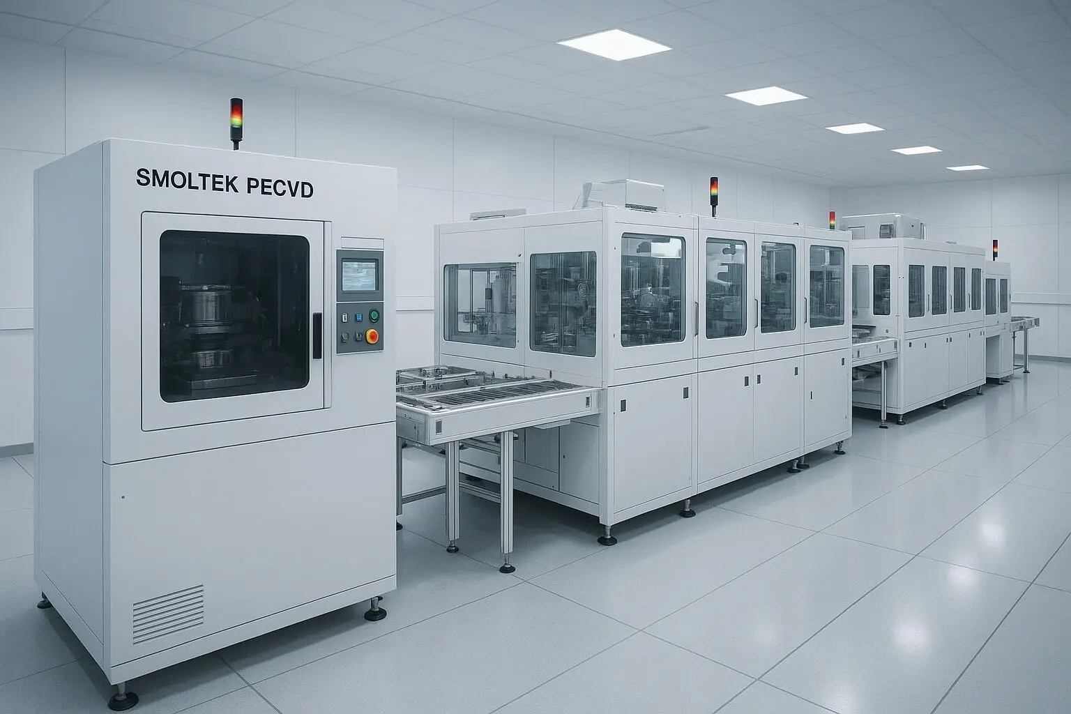
Smoltek Semi is currently optimizing the company’s advanced PECVD system to ensure implementation of its most recent technological innovations in CNF synthesis, enabling compliance with stringent customer requirements, prior to installation at ITRI in Taiwan.