Sign up for our newsletter!
Your data will be handled in compliance with our privacy policy.
Your data will be handled in compliance with our privacy policy.


Smoltek holds unique world patents for technologies that make material engineering on an atomic level possible. Smoltek has solutions that allow continued miniaturization and increased performance of semiconductors, contribute to carbon-free steel production and renewable energy storage, and enable mind control of robotic prostheses. This is a story of how Smoltek came to be.
Thomas Barregren • November 6, 2021
Finn Gramnaes was in the operating room when his daughter was delivered by planned cesarean section. But instead of hearing the newborn announce its arrival into the world with a scream, he heard nothing. “There was a strange silence in the room,” Finn Gramnaes remembers. “It made me terrified, and I froze.”
After what seemed like an eternity, the girl began to scream. But still, something wasn’t right. “I felt there was something in the room that…,” says Finn Gramnaes without finishing the sentence.
Eventually, he got to see his long-awaited baby girl. He was filled with relief and love at the sight of her. She was wonderful. But he also realized that life had taken an unexpected turn. She had a severely deformed right leg. The knee joint was missing as well as the tibia, and the foot was twisted.
After more than six years of well-meant but unsuccessful attempts to reconstruct the knee joint and tibia, the girl’s parents faced a life-changing decision. Sacrifice their daughter’s childhood for more lengthy and painful attempts at reconstruction. Or persuade her to cut off the leg above the non-existent knee joint.
After much deliberation, they persuaded the girl to amputate. “But it did not go as expected,” says her father. When he convinced his daughter to amputate, he didn’t know there were no knee joint prostheses for children. “Instead, they handmade something, with basically a hinge,” he explains.
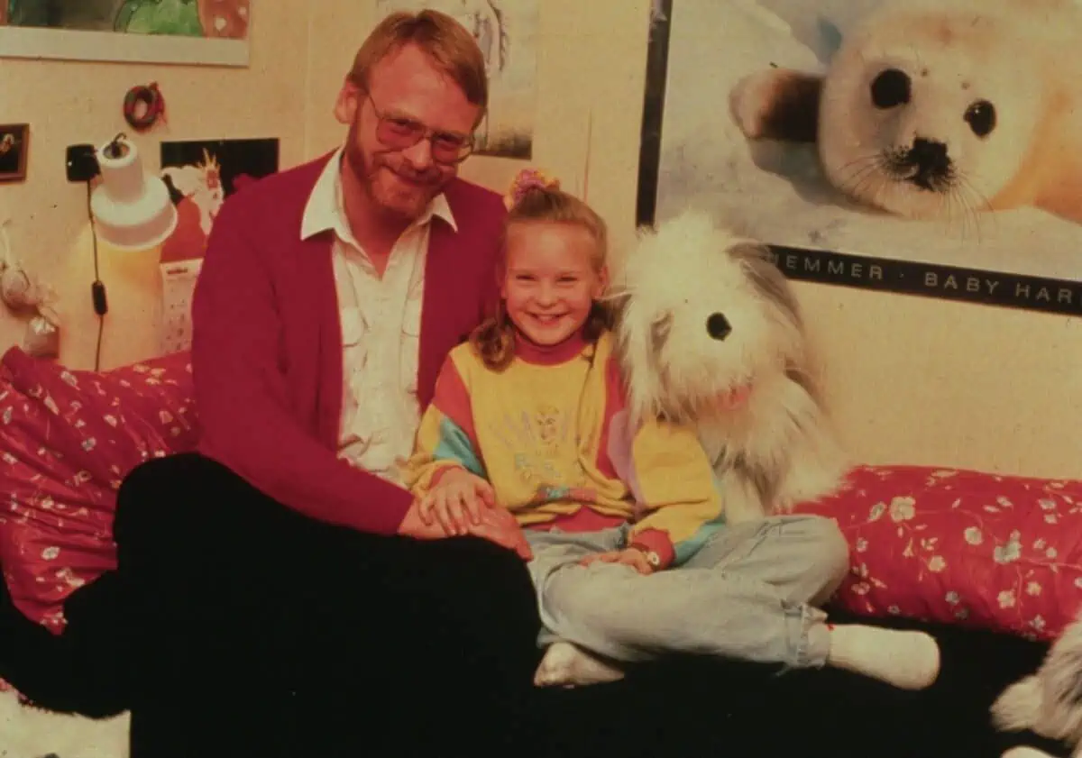
The girl stumbled and fell frequently and often came home with abrasions all over her body. “She was scared and insecure. It was mentally bad for her,” says her father. He experienced terrible remorse for “tricking” his daughter into something that didn’t work out. “We can fly to the moon, but we can’t make knee replacements for children,” he says.
Finn Gramnaes took matters into his own hands. In the evenings, until late at night, and every weekend, he studied anatomy and experimented with designs that mimic a knee joint’s movements and force distribution. His efforts paid off, and he could give his daughter better and better prostheses.
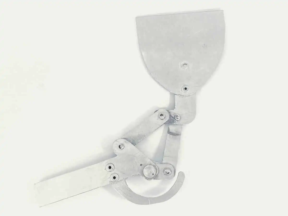
Artificial knee joint
Finn Gramnaes continued to develop his prosthesis. In April 1990, he applied for patents for his “artificial knee joint” and an “artificial foot.”
For more people to benefit from his prostheses, he looked for business partners with good access to capital and a large market. He found them in the United States. Together they founded Century XXII Innovations Inc. in Michigan, where many advanced contract manufacturers serve the aviation industry. Finn Gramnaes became responsible for the development and industrialization of his knee and foot prostheses.

Meanwhile, in Bangladesh, Mohammad Shafiqul Kabir was studying science. Shafiqul—called Shafiq by friends—nurtured a desire to study abroad.
When his studies at the university were coming to an end, he tried to figure out what to do next. He contacted the Swedish Embassy to find out which master’s programs might be of interest. “Swedish universities must have good programs, and afterall, the Nobel prize was established in Sweden,” Shafiq Kabir remembers.
A master’s program at the Chalmers University of Technology in Gothenburg caught his interest. It focused on nanotechnology. “I remember thinking: ‘There it is! I’ll give it a shot’,” says Shafiq Kabir and explains: “Nanotechnology was new and very hyped at the time.”
Shafiq Kabir arrived in Sweden on a sunny day in August 1998. Two years later, in 2000, he graduated with a Master of Science degree.
Shortly after that, Shafiq Kabir was offered doctoral student employment at the Department of Microtechnology and Nanoscience at the Chalmers University of Technology. He was delighted. Since childhood, he had dreamed of doing research.
Shafiq Kabir began this new chapter in his life in the area of molecular electronics but eventually moved to research on carbon nanostructures. In particular, he studied how carbon nanostructures can be made compatible with the manufacturing process of semiconductors. His supervisor, Professor Peter Enoksson, was pioneering and leading in that area.
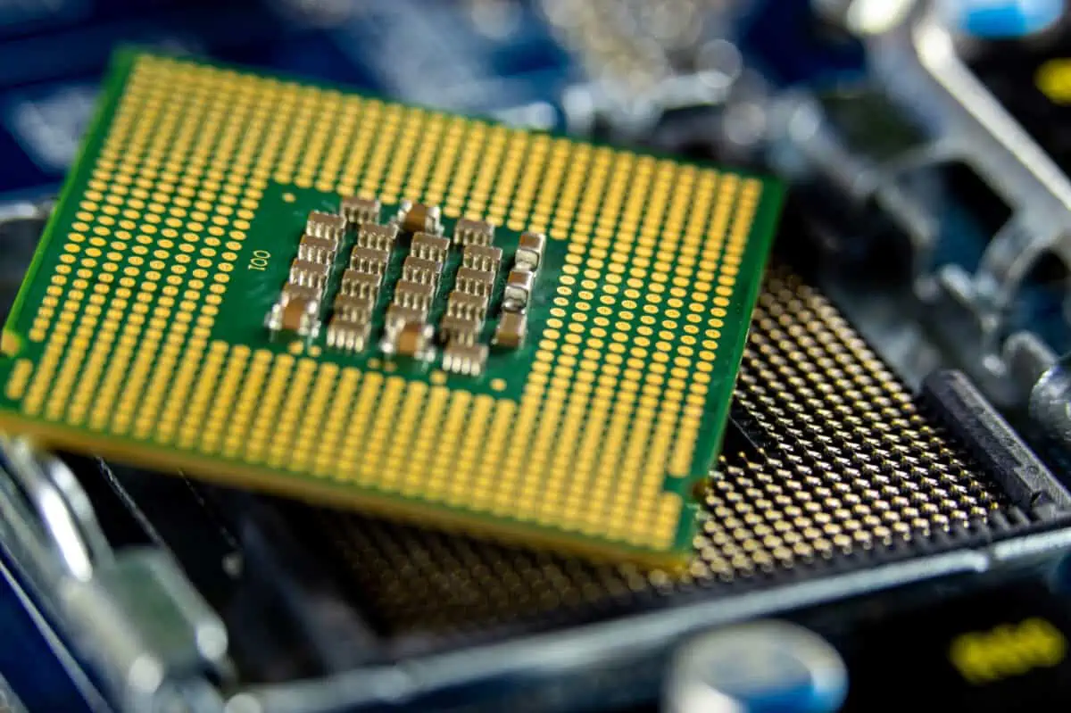
A semiconductor is a material that conducts electric current, but not very well except in areas that are doped. By doping adjacent regions in different ways, a transistor is obtained. It’s an electronic component that can, among other things, turn the power on and off—making ones and zeros—which is fundamental to all digital technology.
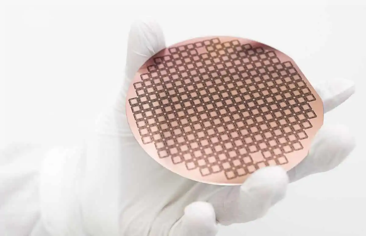
An integrated circuit, or chip in everyday language, is obtained by making many transistors on a single semiconductor wafer and connecting them. A computer’s microprocessor (CPU) and random access memory (RAM) are examples of chips.
Chips, and therefore semiconductors, are in every electronic gadget around you. Usually, chips are made of silicon using a technology called CMOS.
Shafiq Kabir’s research at the Chalmers University of Technology was about using carbon atoms to create small structures directly on CMOS semiconductors. He had to tackle many challenges.
One challenge is that the structures we are talking about are extremely small. They are measured in nanometres (nm). That’s why they are called nanostructures. It is difficult to understand how small they are. But imagine taking one of your hairs and splitting it lengthwise, and then dividing each half again and so on until you have about 50,000 strips of your single hair strand. Each such strip is now about one nanometre in diameter. How can structures that are so incredibly small be built with precision? That was one of the questions Shafiq Kabir searched for an answer to.
Another challenge is that CMOS semiconductors break down at the temperatures needed to fabricate nanostructures. To make it possible to fabricate nanostructures directly on CMOS semiconductors, the fabrication temperature must be lowered by several hundred degrees. But how? That was another of Shafiq Kabir’s research questions.
One form of a nanostructure, in particular, attracted the interest of Shafiq Kabir: carbon nanofibers (CNFs). They have many unique material properties that are interesting in all sorts of contexts.
Carbon nanofibers are surprisingly durable and can be used as a support or reinforcement bar (“rebar”) for materials that become brittle at small sizes. They can also be used as miniature spacers between layers of materials. Or as needles that make microscopic holes in membranes.
Carbon nanofibers are very good at conducting heat—but only in one direction. That property can be used to solve one of the biggest problems as more and more transistors are squeezed onto a chip: Heat dissipation. A chip can become madly hot, shortening its lifespan and increasing the risk of failure. But carbon nanofibers from the chip to the capsule that encloses the chip can effectively dissipate the heat.
And it’s not just heat that carbon nanofibers conduct efficiently, but also electricity. That’s why they can be used as contacts and conductors on chips instead of soldering copper contacts and conductors. The good conductivity, combined with their small size, also opens up the possibility of connecting biosensors directly to individual nerve cells.
But above all, carbon nanofibers arranged in rows and columns can be used to multiply a surface area. Each carbon nanofibre increases the surface area by ? times its diameter times its height. So a “forest” of carbon nanofibers will grow the surface area thousands of times.
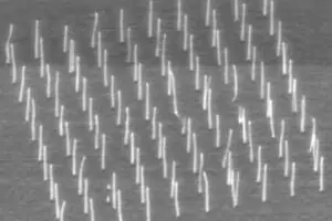
Imagine a square surface with a width and height of one millimeter. It can easily hold 100,000 rows and as many columns of carbon nanofibers that are 5 nanometres in diameter and 50 micrometers in length. The surface area of those carbon nanofibers increases the total surface area 7 855 times. In other words, with carbon nanofibers, you can easily shrink an area of 88 × 88 millimeters to just 1 × 1 millimeters.
This ability to increase the surface area many thousandfolds is beneficial in various applications. For example, with carbon nanofibers coated with titanium on the surface of a titanium implant, the implant’s surface area increases, making it easier to grow together with bone. Another example is the miniaturization of capacitors.
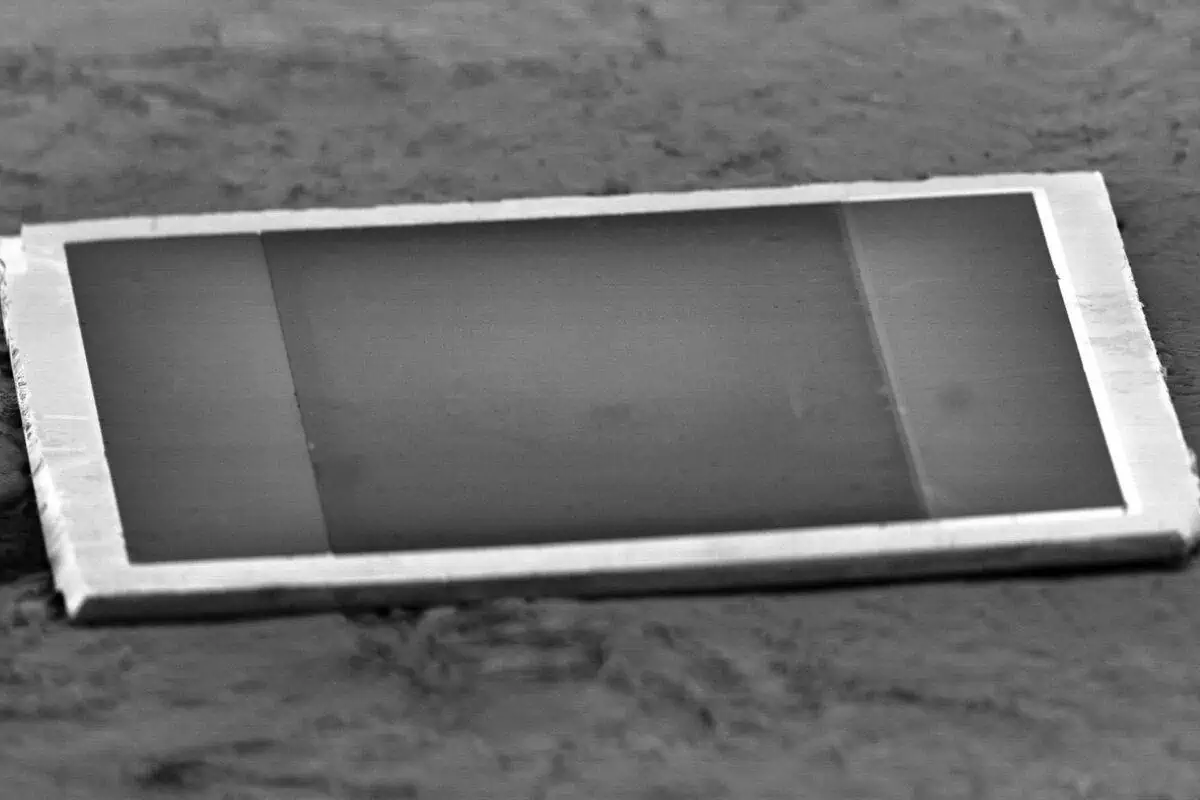
Carbon nanofibre capacitors
A capacitor is an electronic component that temporarily stores energy in the form of an electric field between two separated conductive surfaces. A “forest” of carbon nanofibers provides a lot of surface areas between which energy can be stored in a tiny space. Therefore, capacitors with carbon nanofibers can be made much smaller without degrading their ability to store energy (capacitance).
This is especially useful in chip applications, where capacitors are needed very close to—or preferably on—the chip to dampen the noise that results when thousands of transistors rapidly turn the power on and off to make ones and zeros. The dampening effect comes from the fact that it takes a little while to charge and discharge a capacitor.
However, all these exciting applications of carbon nanofibers require the ability to manufacture them to a specific diameter and length, place them with extreme precision, and do so at a temperature that does not damage the substrate. How to achieve this was the focus of Shafiq Kabir’s research.
His research efforts bore fruit, and in 2005, while finishing his Ph.D. thesis, he started Smoltek to develop the methods further to make them available to the industry. He was accompanied by his Ph.D. advisor, Professor Peter Enoksson.

When Peter Enoksson was offered a chair at the Department of Microtechnology and Nanoscience at the Chalmers University of Technology, he gladly accepted the professorship. He started in October 2001.
He came to work closely with Stefan Bengtsson (now President and CEO of the Chalmers University of Technology) and Eleanor Campbell (who currently holds a Chair of Chemistry at the University of Edinburgh). Their common area of interest was carbon nanostructures. One of the Ph.D. students who also worked on this was Shafiq Kabir.
“Shafiq was very much into applying ‘help layers’ to control where carbon nanostructures grow and to make them faster and more controlled,” Peter Enoksson remembers. Peter Enoksson became Shafiq Kabir’s supervisor.
“We saw many applications of technology and thought it would take over everything,” recalls Peter Enoksson. They called it “the new electronics.”
But they also realized that it had to be made compatible with CMOS—the predominant manufacturing method for semiconductor devices. It had to be possible to manufacture the carbon nanostructures at temperatures that CMOS can withstand—which is much lower than needed to create carbon nanostructures. So this became the focus of their further research.
When Shafiq Kabir later founded Smoltek, Peter Enoksson, Stefan Bengtsson, and Eleanor Campbell became the company’s scientific advisors. And when Smoltek raised seed capital from Chalmers Innovation (now Chalmers Venture), a business incubator associated with the Chalmers University of Technology, Peter Enoksson was involved in investing in the company.
“Shafiq and I thought Smoltek would be huge in just a few years,” says Peter Enoksson with a laugh. Because it turned out not to be as easy as they thought. Despite unprecedented results and excellent properties, it was difficult to convince the electronics industry.
After a few years, it was high time to bring industry experience to the board of directors. The question went to Finn Gramnaes—the father who built a knee prosthesis to help his daughter and then took it to the world market.
In the same year as Shafiq Kabir began his doctoral studies, the company that Finn Gramnaes co-founded in the US was sold to the Icelandic prosthetics manufacturer Össur. Finn Gramnae’s company had received many takeover offers. Eventually, the bids were so high that some of Finn’s senior partners decided it was time to sell.
Finn was now without a job but with a good deal of money in his pocket. He spent a lot of time in Spain, played golf, went to cocktail parties, and tried to live the life expected of someone who had made an exit and was financially independent. But something was missing in his life.
Finn Gramnaes wanted something tangible to do—something that helped others and gave him meaning in life. So he started to help other innovators and entrepreneurs develop their businesses.
Finn Gramnaes had some good contacts in the financial world. They offered their contacts in the hope of sharing risk with someone with money. In this way, Finn came to sit on the boards of a wide range of businesses.
“I was looking for a company that really could contribute to humanity,” Finn Gramnaes says. But years passed without him finding the “right” company. He did, however, learn some hard lessons.
But one day, he found on his desk a document that would change everything.
“One day, someone gave me a text by Smoltek,” Finn Gramnaes says. “It ‘clicked’ when I read it, and I thought, ‘Wow! There it is.’”
Smoltek had a pending patent that covered many application areas. There were many thoughts and visions about what was possible to do with it. “I saw the possibilities and was extremely fascinated,” says Finn Gramnaes. “Smoltek’s technology has the potential to solve many of the problems I encountered during my journey developing prostheses.” He adds: “If I hadn’t made that journey, which made me realize that there is a lack of advanced technology in several areas, I probably wouldn’t have fallen for Smoltek.”
So when Chalmers Innovation asked him if he would consider joining Smoltek’s board, he accepted without hesitation. Eventually, he and Peter Enoksson bought out Chalmers Innovation and became the company’s largest shareholders.
Smoltek’s business concept is to license the technology in various degrees of refinement. From the most basic level, that can be used in industrial research projects, to finished applications, such as carbon nanofibre capacitors.
The business model is to seek partnerships with companies and organizations that want to evaluate or use Smoltek’s technology.
The focus now and in the future will be on creating more and deeper relationships with partners. And not least broaden the search for partners.
Until recently, Smoltek has only focused on the semiconductor industry, but since the formation in autumn 2020 of the subsidiary Smoltek Innovation, the search for partners in new sectors has gathered pace—not least in green energy and green industry.
There are two reasons for Smoltek’s broadening. First, Smoltek’s core technology, for which it holds a world patent, is comprehensive and can be used in many and diverse industries far beyond the semiconductor industry.
The second reason is that the semiconductor industry is very conservative and cautious. It is not surprising. Companies in the industry are making huge investments, counted in billions of dollars, which increase dramatically with each new generation of CPUs and other semiconductor components. Therefore, companies are extremely cautious about what technology they bring in. It has to be established and already proved itself in the real world.
The last reason is also why Smoltek has chosen to focus on carbon nanofibre capacitors. It gives Smoltek a chance to show what the technology is capable of, in a way visible to the semiconductor industry, but with no risk for them.
Many chips have attached capacitors that compete with connectors for space. If the capacitors can be made smaller, the chip can be made smaller or have more connectors.
Smoltek’s strategy is to help the world’s largest capacitor manufacturers use carbon nanofibers to produce capacitors that take up less surface area and, more importantly, less height than the miniaturized capacitors available today.
In this way, Smoltek’s technology is battle-tested in a way that is “harmless” to the semiconductor industry but visible to them. In parallel, Smoltek talks with all major companies in the semiconductor industry to convince them to dare the leap.
Once the carbon nanofibre capacitors have proven themselves as discrete components, the next step will be to move them into the chip. The final goal is to build them directly on the silicon. Smoltek already has the technology for this.
Once on silicon, Smoltek can help the semiconductor industry with many other things too. For example, creating chips with multiple silicon layers where Smoltek’s carbon nanofibers can act as miniature spacers, solder joint reinforcement bars, or electrical conductors. Smoltek’s technology can also dissipate the heat generated inside the chip, thereby making cooling easier.

Smoltek has focused on the semiconductor industry from the very beginning. It came naturally; Shafiq’s research was about creating carbon nanostructures on CMOS semiconductors, and the semiconductor industry needs new solutions to keep doubling the number of transistors every two years.
But Smoltek’s technology has many applications far beyond the semiconductor industry. Therefore, Smoltek has moved the semiconductor endeavor into its own business unit, called Smoltek Semi, and added a new business unit, called Smoltek Innovation, with the mission to pursue other applications.
Just as Smoltek Semi has strategically chosen to focus on carbon nanofibre capacitors, Smoltek Innovation has strategically placed hydrogen production in its focal point. Hydrogen has emerged as the key to making heavy industry carbon-free and storing renewable energy. Two application areas of immediate vital importance.
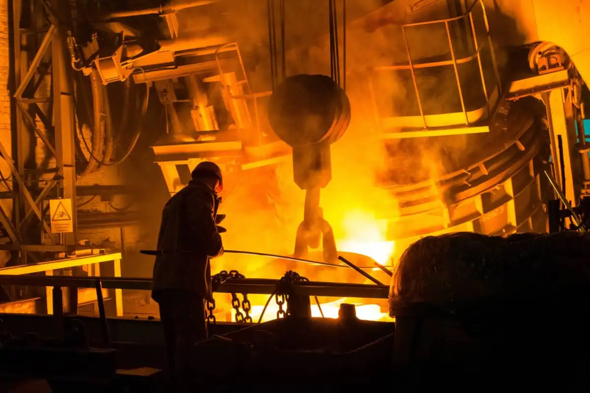
In heavy industry, projects are underway to reduce their use of fossil fuels and greenhouse gas emissions.
In Sweden, for example, the mining company LKAB, the steel manufacturer SSAB and the energy company Vattenfall are working on a joint project to develop fossil-free steel. Hydrogen gas has an essential function in this context; the gas replaces coal and coke in steel production.
The technology can reduce carbon dioxide emissions from the Swedish industry by a third, and in the future, help reduce emissions from iron and steel production worldwide.
However, there is a catch. If the steel is to be fossil-free, the hydrogen must be produced in a renewable way.
Hydrogen can be produced by running electricity through water. In this process, water, consisting of two hydrogen atoms and one oxygen atom, is splintered into hydrogen gas and oxygen gas.
But for this hydrogen production to be fossil-free, the electricity used must also be fossil-free and preferably produced from renewable sources. Thus, the production of hydrogen must use electricity produced by solar, wind, or water.
Such electricity is not always in constant supply; the sun goes into the clouds, the wind slackens, and water reservoirs dry up. So the process of producing hydrogen must work in the presence of an intermittent power supply.
There are two main ways to produce hydrogen by running electricity through water.
The oldest and most conventional way of producing hydrogen is alkaline electrolysis. In this process, lye (potassium hydroxide or sodium hydroxide), which is highly corrosive, is added, and electricity is applied through two electrodes made of a nickel alloy. These electrodes are separated by a membrane which allows hydroxide ions (OH-) to flow through, on their way from one electrode to the other, while separating the hydrogen gas produced at one electrode from the oxygen gas produced at the other.
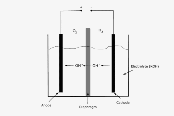
This technique has several disadvantages. Mainly is the low efficiency. The energy value of the hydrogen generated is only 65% of the energy supplied. In addition, the method works poorly when the availability of electricity varies.
A better technique is polymer electrolyte membrane (PEM) electrolysis. Its main advantages are high efficiency, currently upwards of 80%, and expected to reach 86% by 2030. In addition, the method works even when the electricity is fluctuating, making it suitable for use with renewable energy sources such as solar and wind.
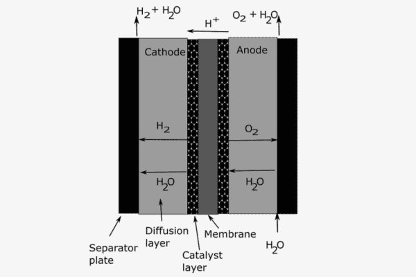
But the electrodes immersed in water on either side of the membrane must be coated with the scarce and precious metals platinum and iridium. For comparison, gold is 40 times more abundant in the Earth’s crust than iridium. The annual production is just three tonnes.
This is where Smoltek’s technology comes in.
Smoltek’s technology allows particles of the rare and precious metals to be placed at the tip of carbon nanofibers, which in turn are placed in a way that maximizes exposure. In this way, the electrodes can be made up to three times more efficient while reducing the amount of precious metal needed. This, in turn, can lead to savings of up to 30 percent for hydrogen production plants.
The same method can be used for energy storage.
A sore point for renewables like solar and wind is the difficulty of storing the energy produced. Solar energy can be stored in batteries for short periods, but to save the energy produced during the many hours of sunshine in summer for the dark and cold season requires an entirely different storage technology. This is where hydrogen comes in.
When renewable sources produce excess electricity, the surplus is converted into hydrogen stored for later use. The oxygen emitted as a by-product is released or used for various purposes.
The hydrogen thus created can then be used in fuel cells. They produce electricity from hydrogen, with only water vapor as a by-product.


Smoltek was founded in 2005 by Shafiq Kabir. It is his research and innovations that are the foundation on which Smoltek is built. He left Smoltek in January 2013 to try his wings as a consultant but returned in October 2015. In January 2021, he transitioned to an advisory role to free up time for his Executive MBA studies and personal projects.

Peter Enoksson, Professor of Microtechnology and Nanoscience at the Chalmers University of Technology, has been on board all the way. His journey began even before Smoltek was founded. At his department, Shafiq Kabir received his master’s degree, and it was under his supervision, Shafiq Kabir earned his Ph.D. Peter Enoksson contributes knowledge, networks, and not least contacts with promising researchers in the field.

Finn Gramnaes also got on board early. When Smoltek’s time in the incubator was over, he and Peter Enkosson bought out Chalmers Innovation and became the company’s largest shareholders.
As active owners, Finn Gramnaes and Peter Enkosson have taken on the task of lifting their gaze to see the forest for the trees. And what they are glimpsing at the end of the forest is an environmentally friendly product line—made possible with Smoltek’s technology.
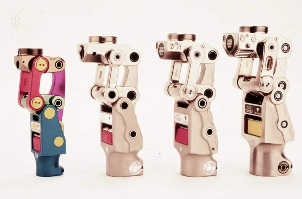
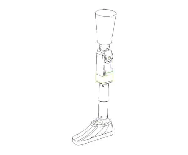
In the early 2000s, when Finn Gramnaes was still looking for something meaningful to do, and his daughter Lisa had just graduated with a bachelor’s degree in mechanics, the two began developing an artificial leg. Their ambitious goal was to create a prosthesis that even better mimics human movement using advanced sensor technology and electric motor technology.
“We participated in some university projects and learned bit by bit how to build a robotic leg prosthesis,” Finn Gramnaes says. They were eventually able to patent an advanced robotic prosthetic leg.
But the effort was in vain. The prosthesis could not be made; the technology wasn’t commercially available. “We were way ahead of our time,” Finn Gramnaes says, adding, “The battery technology was not developed. There were not the kind of motors that were needed. Microprocessors needed to be smaller and more powerful. In particular, sensors were needed that could detect different movement patterns and surfaces under real-life conditions.”
Shortly after Finn Gramnaes realized that the advanced technology he needed was not available, someone gave him the text written by Smoltek—the one that made him cry out, “Wow! There it is.”
What clicked when he read about their technology was the potential to solve many of the problems he and his daughter had identified. One example is the possibility of developing biosensors. Carbon nanofibers are significantly smaller than cells. Therefore, they can be used to connect individual neurons to electronics electrically. Something necessary to control a robotic prosthetic leg with only the mind.
Precisely this, creating a tiny chip with carbon fiber sensors, signal amplification, and an electrical interface, is among the things Smoltek Innovation is looking at right now, in 2021. So maybe tomorrow’s parents, who in the past had to persuade their children to remove a body part, can instead comfort their child with the fact that there are robotic prostheses that, thanks to Smoltek, can be controlled with the power of thought.
May the force be with them.
Your data will be handled in compliance with our privacy policy.
IR Blog Posts

September 5, 2024
Smoltek’s focus on qualified research places it firmly in the Explorer quadrant of the R&D Evaluation Matrix, a model for assessing a company’s research and development strategy. Discover why this matters to investors and how Smoltek translates groundbreaking research into valuable business opportunities.
IR Blog Posts

April 14, 2025
Taking a breakthrough technology from the lab bench to the world market often requires collaboration with large industrial enterprises. In this interview, Ellinor Ehrnberg, president of Smoltek Hydrogen, explains how the company aligns its own development with that of potential buyers while navigating the complex journey from initial interest to strategic partnership.
News
June 18, 2025
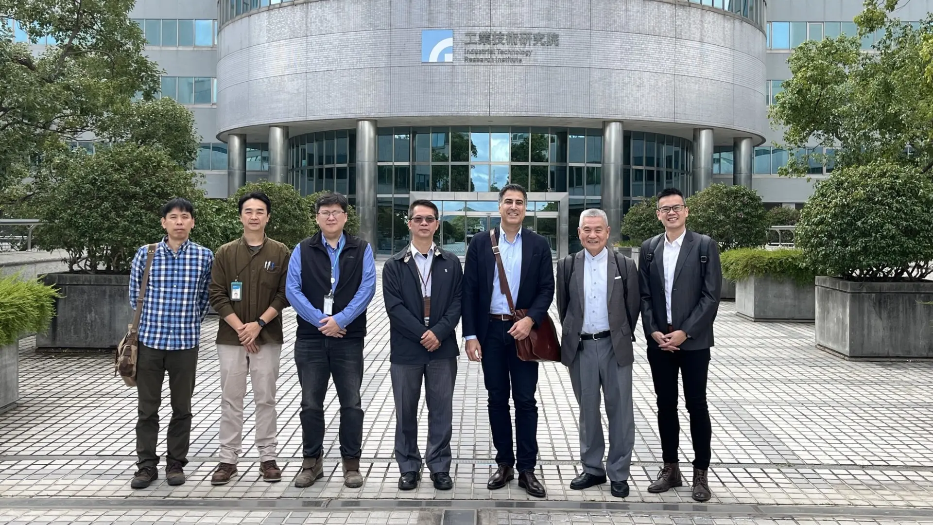
Smoltek Semi has initiated the signing of a technical service agreement with the Taiwanese Industrial Technology Research Institute (ITRI) that enables low-volume production of Smoltek's propriety CNF-MIM capacitors.
IR Blog Posts

July 30, 2025
The recently signed technical service agreement between Smoltek Semi and the Industrial Technology Research Institute (ITRI) of Taiwan changes how CNF-MIM capacitors will reach the market. This partnership delivers the validation and manufacturing capabilities needed to transform laboratory breakthroughs into commercial reality.
IR Blog Posts

October 11, 2024
Our innovative “zapping” method drastically reduces development time and costs, enabling us to advance CNF-MIM technology faster and making Smoltek Semi’s technology even more attractive to potential buyers. Read on to see how this new process strengthens our position and shortens our path to market.
IR Blog Posts

October 1, 2024
Smoltek Semi has developed a new material for use in CNF-MIM capacitors. The new material increases capacitance by more than three times and reduces leakage current by 50 percent. In this article, we examine what this means and why it is good for shareholders and investors.