Sign up for our newsletter!
Your data will be handled in compliance with our privacy policy.
Your data will be handled in compliance with our privacy policy.

Smoltek keep growing its proprietary technology platform. In the beginning of May 2020 patent No. 58 was granted. The patent is connected to our helplayer family.
The company’s third granted patent in 2020 is a European (EPO) patent. It is an invention that relates to how to grow nanostructures on substrate without destroying the underlying materials for example CMOS circuit elements, sensors etc., which may be sensitive to such a growth process.
The patent covers an essential aspect of method of producing nanostructures on a substrate where the surface constitutes both conducing and non-conducting structures and devices out of the same.“This new patent covers essential aspects of a production method that enables growth of nanostructures on any given surface including presence of sensitive circuit elements underneath. The beauty of the technology lies in its simplicity. It is easy to implement in, and compatible with volume production set-ups. The new patent adds to our growth-related part of our patent portfolio, and provides additional protection of our key technology.”, says Shafiq Kabir, CIO at Smoltek.
Smoltek’s patent portfolio now globally comprises 58 granted patents. Read more about our IP and patents.
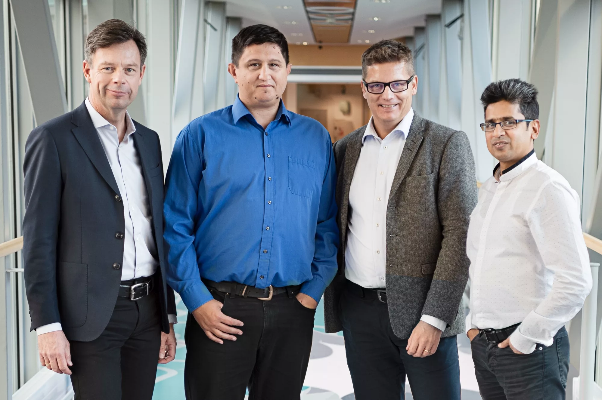
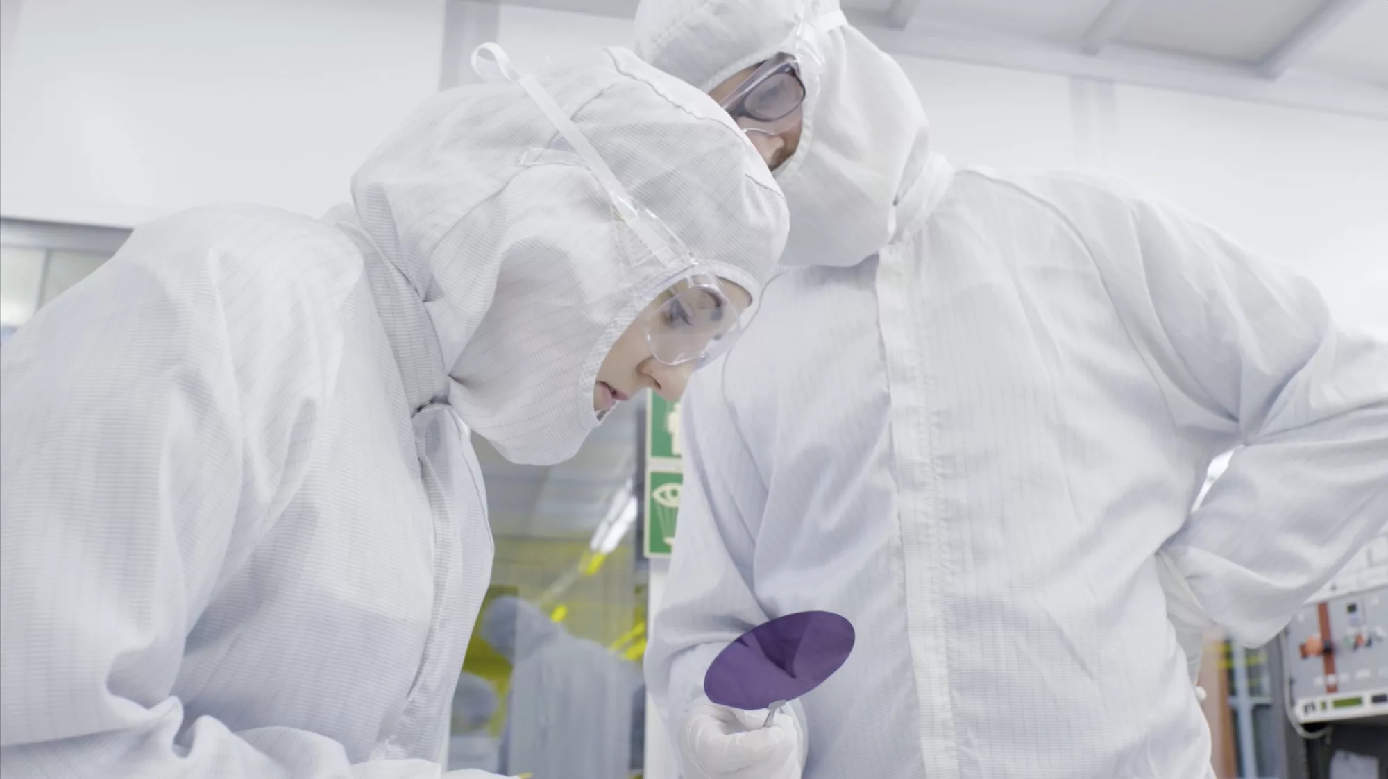
Image: Smoltek CEO, CTO, COO and CIO
Your data will be handled in compliance with our privacy policy.
News
February 24, 2026
An independent, third-party reliability test of our CNF-MIM capacitor technology has confirmed the reliability results communicated on February 5, 2026. The independent validation, performed by a major capacitor manufacturer, also reduces technical risk in the commercialization process and strengthens Smoltek’s credibility in ongoing negotiations with industrial partners.
News

February 5, 2026
Smoltek’s CNF-MIM capacitors demonstrate excellent stability in a new 1,000-hour life test at 85°C under applied 2 volts. No degradations were observed, and the capacitors exhibited more than 1,000 times lower current leakage compared to the previous life test.
News

November 20, 2025
We have launched a podcast about materials technology and investments in general and our disruptive carbon nanotechnology in particular.
News
November 17, 2025
Smoltek Semi is currently optimizing the company’s advanced PECVD system to ensure implementation of its most recent technological innovations in CNF synthesis, enabling compliance with stringent customer requirements, prior to installation at ITRI in Taiwan.
News
November 5, 2025
Smoltek Semi has reached an important technical milestone in the development of the company’s carbon fiber-based CNF-MIM technology. The capacitors have successfully passed a 1,000-hour high-temperature durability test, confirming the robustness of the technology for advanced applications.
News
October 24, 2025
Smoltek Semi has acquired a plasma-enhanced Atomic Layer Deposition (ALD) system to implement its advanced dielectric stack on carbon nanofibers. The system will significantly reduce the iteration time of coating processes while enabling innovation and IP generation in dielectric stack technology for carbon nanofiber electrodes.