Sign up for our newsletter!
Your data will be handled in compliance with our privacy policy.
Your data will be handled in compliance with our privacy policy.

Carbon nanofibers is a supermaterial. It is stronger, more elastic, and lighter than steel. It conducts heat and electricity better than metals. And it can be used to thousandfold the surface of materials. Let’s take a closer look at these tiny fellows.
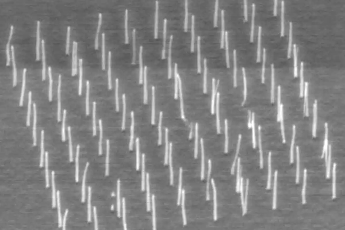
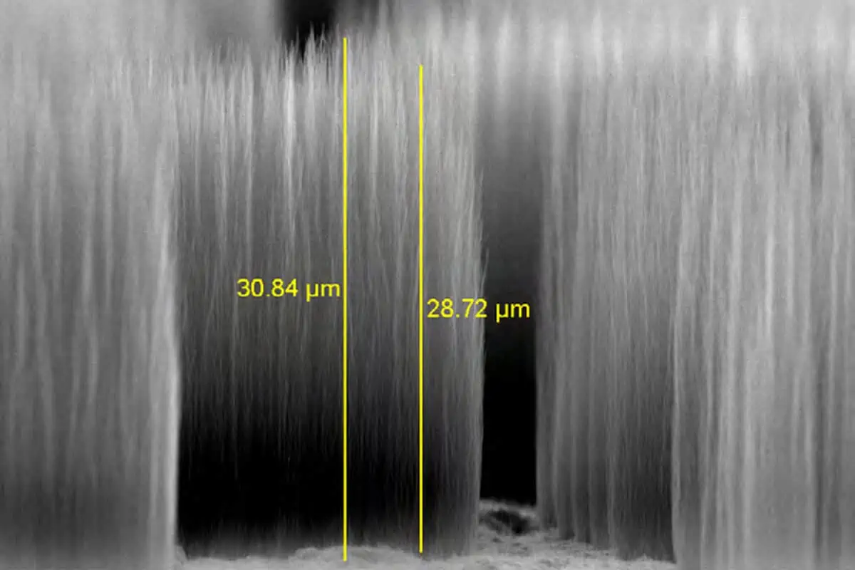
A carbon nanofiber (CNF) is a carbon-made material so thin that its diameter is measured in nanometers. Its length is many times longer than its diameter. Carbon nanofibers have diameters in the range of 5–500 nm and lengths in the range of 1–200 μm.
A nanometer (1 nm) is one-thousandth of a micrometer (0.001 µm). That’s so tiny that only three free carbon atoms fit on a straight line of that length.1 To get an idea of how extremely small that is, let’s imagine a hair strand. If you split it lengthwise, and then split the two halves again, and then repeat this over and over again until you have 70,000 strains from that single strand, then each of them is about 1 nanometer thick.2
Carbon nanofibers is ten times stronger than the strongest steel in the world (maraging steel) and up to a hundred times stronger than ordinary steel.
The tensile strength of carbon nanofibers is a mind-boggling 30 GPa.
Suppose you have a round bar with a diameter of 1 cm and the same tensile strength as carbon nanofibers. Let’s assume you somehow manage to hang a mid-size car from its end. Then you add another, and yet another, and so on until the round bar breaks. Can you guess how many cars were hanging from the round bar before it broke? Two hundred! That’s how strong carbon nanofibers are.
Therefore, carbon nanofiber is an excellent building block at the microscopic level. It can be used as a support or as a reinforcement bar (“rebar”) for materials that become brittle at small sizes. They can also be used as tiny spacers between layers of materials. Or as needles that make microscopic holes in membranes.
If you were going to bend a carbon nanofiber, think again. It requires four times more force to bend or stretch carbon nanofibers than steel. And the little fillet will return to its original shape as soon as you release it—like a rubber band.
The Young’s Modulus of carbon nanofibers varies between 80 and 800 GPa.
Although carbon nanofiber is much stronger than steel, it weighs only a quarter of steel.
The density of carbon nanofiber is between 1.3 and 2 g/cm3.
Imagine a steel cube with sides 10 cm long and a carbon nanofiber cube of the same size. If you put them on separate scales, the one with the steel cube will read 8 kg, while the one with the carbon fiber cube will read less than 2 kg.
Silver and copper are the best heat-conductive metals. Yet they take a beating compared to carbon nanofibers, which can be made to conduct heat more than seven times better.
The thermal conductivity of carbon nanofibers varies between 20 and 3,000 W/(mK) depending on how they are manufactured.
That excellent heat conductivity can be used to solve one of the biggest problems as more and more transistors are squeezed onto a chip: Heat dissipation. A chip can become madly hot, shortening its lifespan and increasing the risk of failure. But the heat can effectively be dissipated by carbon nanofibers between the chip and the capsule enclosing it.
It’s not just heat that carbon nanofibers conduct efficiently, but also electricity. Again silver and copper are the metals that conduct best. Carbon nanofiber is not quite as good, falling between iron and steel.
The electrical conductivity of carbon nanofibers varies from 5⋅102 to 107 S/m. That is, the resistivity varies between 0,1 µΩm and 2 mΩm.
The good conductivity, combined with the small size, opens up the possibility of connecting biosensors made by carbon nanofibers directly to individual nerve cells. Carbon nanofibers can also be used on chips instead of soldering copper contacts and conductors.
An exciting application for carbon nanofibers is as surface coatings to increase the contact area. By growing carbon nanofibers directly on a surface, the contact area can be increased tens of thousands of times.
Imagine a square surface with a width and height of one millimeter. It can easily hold 100,000 rows and as many columns of carbon nanofibers being 5 nanometers in diameter and 50 micrometers in length. The surface area of those carbon nanofibers increases the total surface area 7 855 times. In other words, with carbon nanofibers, you can easily shrink an area of 88 × 88 millimeters to just 1 × 1 millimeters.
Increasing the surface area many thousandfolds is beneficial in various applications. One example is carbon nanofibers coated with titanium on the surface of a titanium implant. The surface area of the implant will increase making it easier to join the bone. Another example is the miniaturization of capacitors.
What makes CNF so special is how the carbon atoms are arranged. To understand how we must first review some basic atomic theories.
Bohr’s classical model of an atom describes it as a nucleus surrounded by shells of electrons. Each shell has room for a fixed number of electrons. The innermost shell has two locations. The following shell has room for eight electrons. And so on. In most cases, the shells fill up from the inside out. When a shell is complete, it is said to be closed. If it’s not complete, it is, of course, called open.
Electrons in the outermost shell are called valence electrons. Only noble gases have valence electrons in a closed shell. They are super stable. All other substances have valence electrons in an open shell, and these can do all sorts of crazy things.
For example, a valence electron in an open shell can attract another atom, and in exchange for it also serve as the valence electron for the other atom. In this way, the two atoms will share an electron. This creates a bond between the two atoms. This type of bond, where the atoms share one or more electrons equally, is called a covalent bond.
A carbon atom has six electrons: Two are in the innermost electron shell (which is therefore closed), and four are in the shell outside (which is therefore open). So the carbon atom has four valence electrons but “needs” four more to close the outer shell. Therefore, free carbon atoms do not become long-lived; they soon find other atoms to create covalent bonds with.
A carbon atom can fill the outer shell by a valence electron, forming a covalent bond with another carbon atom. These, in turn, can do the same. Suppose this is repeated over and over again. In that case, we get a molecule made up of carbon atom after carbon atom. The properties of these carbon atoms depend on how they arrange themselves.
Allotropy is the phenomenon of certain elements that can exist in different forms called allotropes. Carbon has many allotropes.
A three-dimensional array of carbon atoms, where each bond has the same angle to its neighbors, is called a diamond.
Carbon atoms that form hexagonal rings, where adjacent rings share sides and are in the same plane, are called graphene. It looks like a sheet of chicken wire where the knots are carbon atoms, and the threads between them are covalent bonds.
Graphite is layers upon layers of graphene. The layers are held together by quantum dynamic interactions between atoms in adjacent layers called van der Waals force.
Carbon atoms that form five‑, six- or seven-sided rings, where adjacent rings share sides but are not in the same plane, are called fullerene. These occur in many different forms, many of which have their own names. In a sense, graphene is just a special case.
A fullerene that looks like a tube, possibly closed at the end, is said to be a single-wall carbon nanotube (SWCNT) or carbon nanotube (CNT) for short. A multi-wall carbon nanotube (MWCNT) consists of one SWCNT enclosing another SWCNT, possibly enclosing a third SWCNT, and so on. The nested SWCNTs are “glued” to each other by the van der Waals force.
Finally, we have arrived at the carbon nanofiber (CNF), which can be seen as a “modified MWCNT” where each tube is tightened at one end so that they take the shape of a plate, cup, or cone before they are stacked one inside the other.
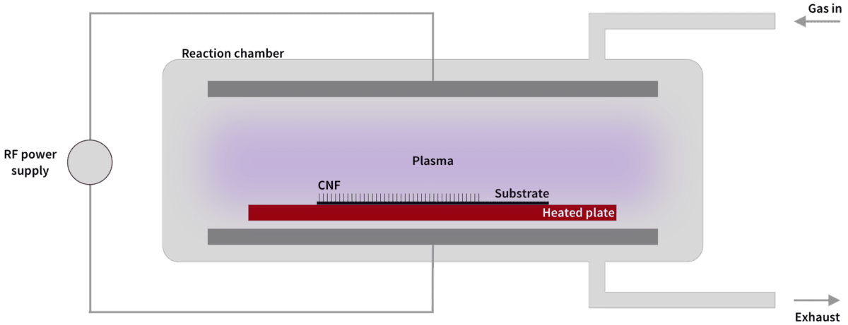
Commercial fabrication of carbon nanofibers is often done with Catalytic Chemical Vapor Deposition (CCVD, or simply CVD). The basic idea is to apply so much energy to a carbon-based gas, in the form of heating or lightning discharges, that the valence electrons are torn loose, releasing carbon ions that can deposit on surfaces prepared with catalytic metal.
Smoltek has developed a patented solution to control with extreme precision where the released carbon atoms settle and how they are formed into carbon nanofibers. This gives us a unique opportunity to tailor carbon nanofibers with desired properties. We have also developed the technology to use comparatively low temperatures (375 °C), which allows our manufacturing technique to be used in production lines in the semiconductor industry.
The following is a simplified description of our manufacturing process, which we call SmolGROW:
Smoltek’s technology works not only with carbon nanofibers. It is possible to create other carbon nanostructures, like carbon nanotubes (CNTs), and also use materials other than carbon.
Do you want to learn more about carbon nanofibers and how they can be used in your application? Contact us and let’s have a chat.
Your data will be handled in compliance with our privacy policy.

With our carbon nanofibers (CNFs) fabrication technology, we develop advanced materials engineering solutions for use in water electrolysis and fuel cells for the hydrogen industry.
Smoltek has developed the world’s thinnest discrete capacitor. You have to stack ten of them on top of each other to reach the same height as today’s industry-standard when it comes to surface-mounted capacitors. The most amazing thing about this microscopic capacitor is its performance. One square millimeter has a capacitance of a whopping 650 nanofarads (650 nF/mm2). Read on for more details.

Carbon nanofibers in hydrogen electrolysis & fuel cells Hydrogen has emerged as a key to store renewable energy and making heavy industry carbon-free. Two application areas of immediate vital importance. The core technologies that make this possible are hydrogen electrolysis and fuel cells. Electrolysis converts electricity into hydrogen, while fuel cells convert the hydrogen back to electricity.

Smoltek holds unique world patents for technologies that make material engineering on an atomic level possible. Smoltek has solutions that allow continued miniaturization and increased performance of semiconductors, contribute to carbon-free steel production and renewable energy storage, and enable mind control of robotic prostheses. This is a story of how Smoltek came to be.

A main goal for Smoltek Semi is to develop an industrial process for mass production of discrete CNF-MIM capacitors at contract manufacturers (foundry), including a specially designed machine for large-scale production of carbon nanofibers.

PhD thesis, Chalmers Univeristy of Technology, 2017.