Sign up for our newsletter!
Your data will be handled in compliance with our privacy policy.

Smoltek has developed the world’s thinnest discrete capacitor. You have to stack ten of them on top of each other to reach the same height as today’s industry-standard when it comes to surface-mounted capacitors. The most amazing thing about this microscopic capacitor is its performance. One square millimeter has a capacitance of a whopping 650 nanofarads (650 nF/mm2). Read on for more details.
Thomas Barregren • November 6, 2021
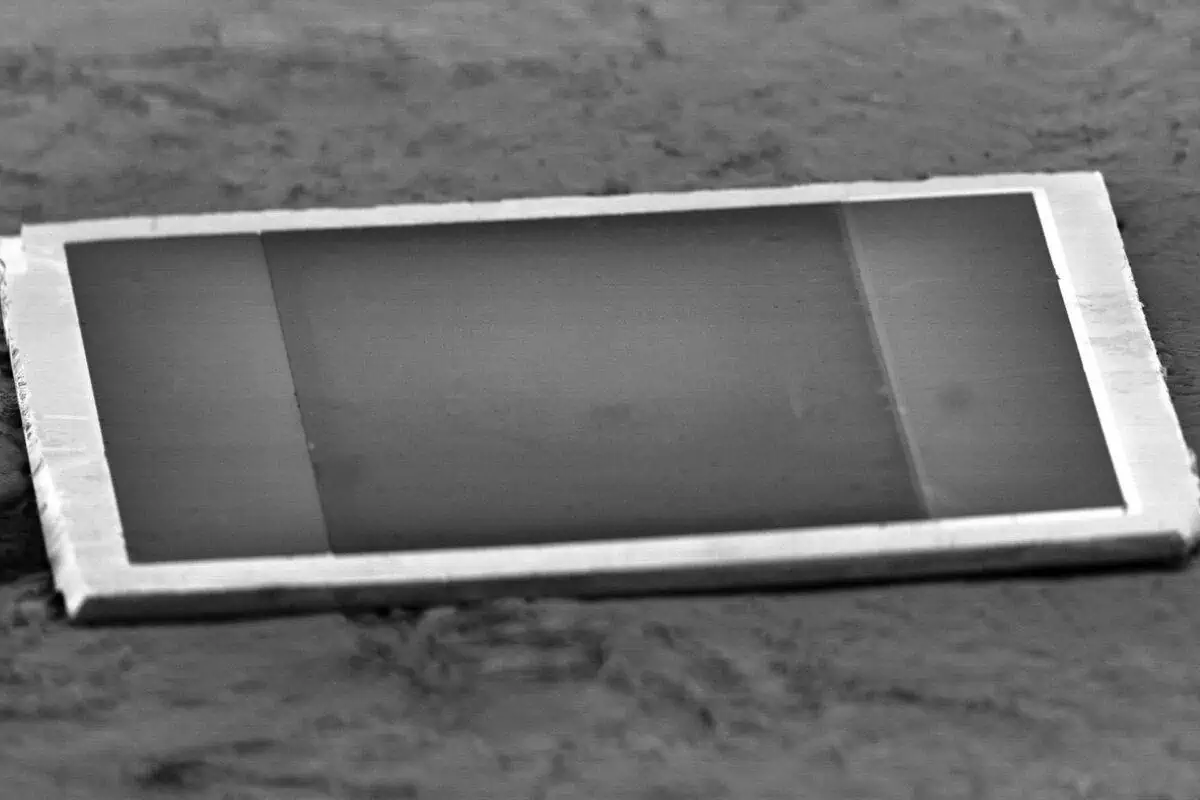
The world’s thinnest discrete capacitor has a total building height is less than thirty micrometers (30 µm). The capacitor itself, without encapsulation, is a mere 0.5 to 10 µm. It can be built directly onto an integrated circuit’s die or built into its interposer. One square millimeter has a capacitance of a whopping 650 nanofarads (650 nF/mm2). Its internal resistance (ESR) is less than forty milliohms (40 mΩ), and its internal inductance (ESL) is below fifteen picohenry (15 pH).
We describe our capacitor as a CNF-MIM capacitor since it is a metal-insulator-metal (MIM) capacitor where carbon nanofibers (CNF) are used to create a much larger surface area hence higher capacitance than the form factor suggest.
A discrete CNF-MIM capacitor has a smaller footprint (area) and much thinner profile (z‑dimension) than any other capacitor with the same capacitance. CNF-MIM capacitors up to more than 650 nF can be made less than 30 µm in height. The actual form factor can be varied according to the design and need.
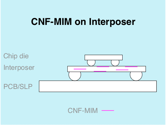
As shown in the illustrations, a discrete CNF-MIM capacitor can be
Discrete CNF-MIM capacitors are compatible with wafer to wafer (W2W) or die to wafer bonding (D2W).
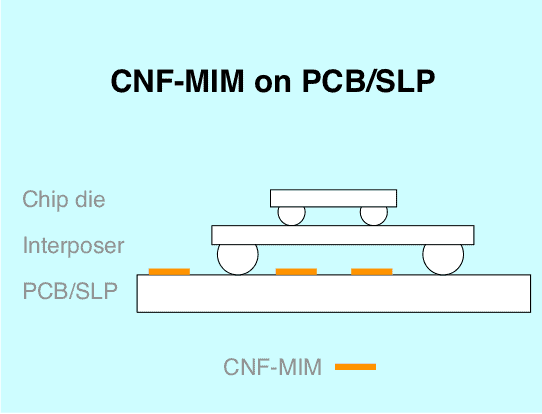
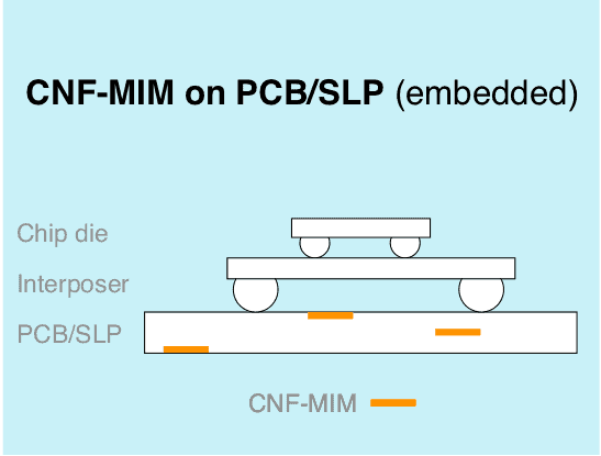
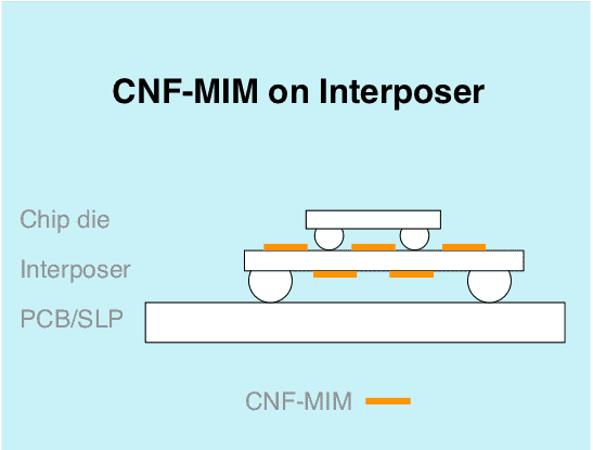
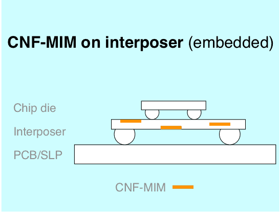
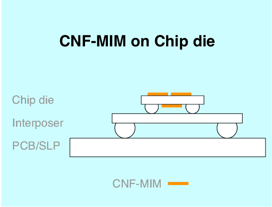
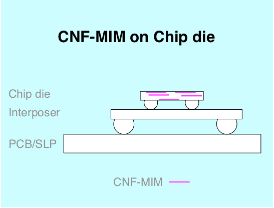
A CNF-MIM capacitor can be integrated directly into chip die or chip interposer. The height of the integrated capacitors is a mere 0.5 to 10 µm. The benefits with integrated CNF-MIM are many:
As shown in the illustrations, a CNF-MIM capacitor can be
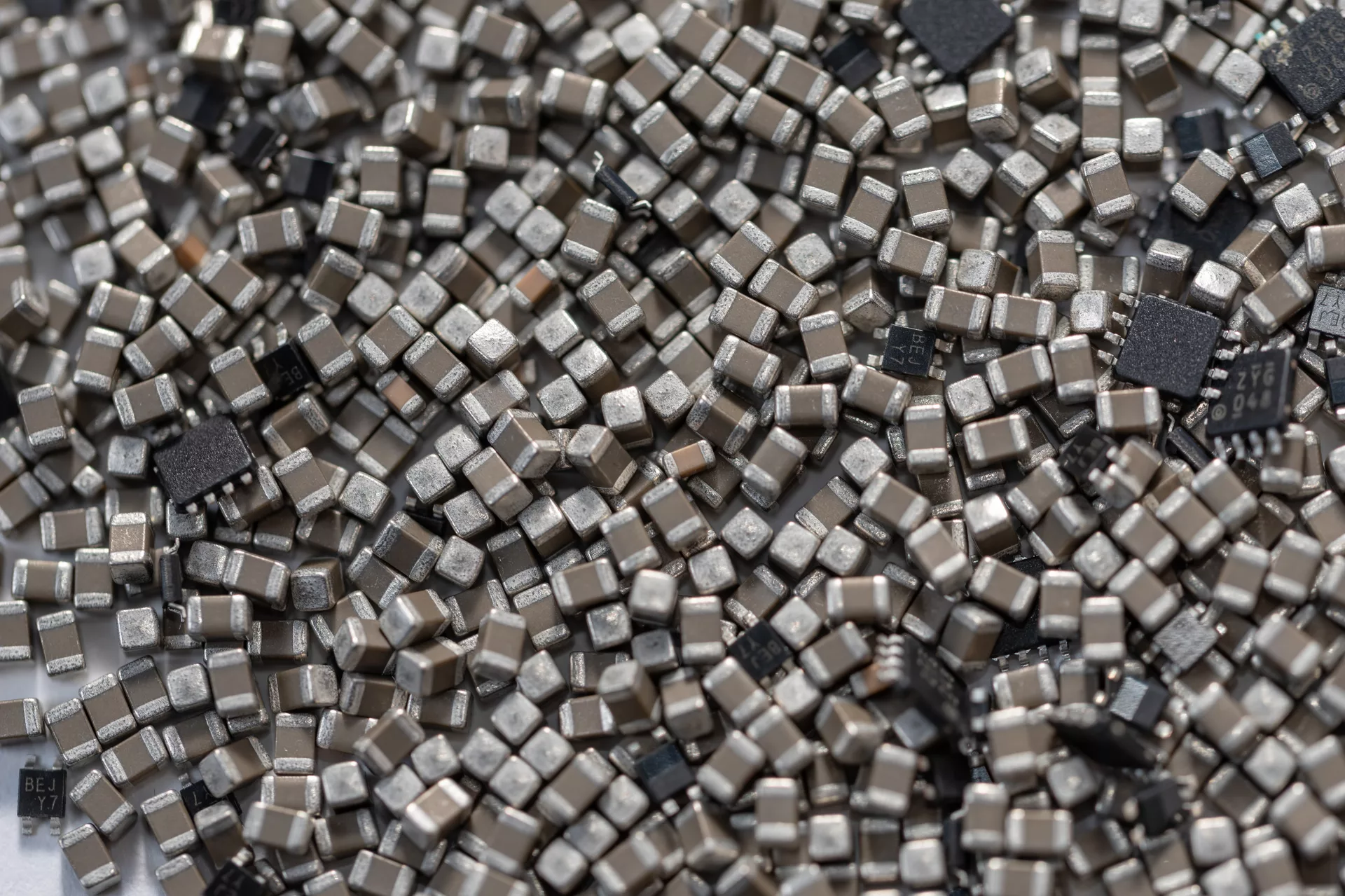
Multilayer Ceramic Capacitors (MLCC) form the industry standard for surface-mounted device (SMD) capacitors. Every year, trillions of MLCCs are built into all kinds of electronic devices. They are 300 µm high. CNF-MIM offers the same capacitance at a tenth of that height.
The miniaturization of electronics is creating a growing need for ever smaller capacitors. And some circuits (such as Apple’s) use capacitors that are state of the art. These use improvements of MLCC and Low Inductance Chip Capacitors (LICCs) and Trench Silicon Capacitors (TSCs), all of which have a height of 80–100 µm.
However, MLCC, LICC, and TSC struggle to go down in height due to materials involved, processing schemes, and the cost of raw materials and processing. At the same time, SiP and SoC continue to become more compact. There is less and less space between interconnects (bumps), and they are getting shorter. To fit capacitors between the bumps, the capacitors must have a smaller footprint and, above all, be shorter—preferably less than 20 µm.
This is the problem that CNF-MIM capacitors solve. They have a much smaller footprint and, above all, a much lower height.
A metal-insulator-metal capacitor, or MIM capacitor for short, has parallel metal plates with a thin layer of an electric insulator between them. The simplest form of a MIM-capacitor is the parallel plate capacitor.
Now, imagine we connect a battery to a MIM-capacitor. Since no current can pass through the isolator, the electrons pushed into the plate on one side of the isolator build up a positive charge. The electrons pulled out from the plate on the other side of the isolator build a negative charge. The charges increase respectively decrease the electrical potential on the plates. The buildup continues until the difference between the potential is the same as the battery’s voltage. The difference in charge between the two plates creates an electric field between them.
When the battery is removed, the electric field remains since the charges have nowhere to go. Only when the capacitor is connected to a closed circuit, the charges in the capacitor can flow. The capacitor thus stores energy in the form of an electric field.
Any material that does not conduct current can be used as an electrical insulator. But generally, dielectric materials are used.
Dielectric material consists of atoms whose electrons cannot move freely enough to carry current like all insulators. But unlike materials that are commonly called insulators, such as ceramics, dialectic materials become polarized in the presence of an electric field. They have electrons that are so free to move that the electric field pulls them away from the nucleus. Figuratively, the atom becomes elongated, with one end being negatively charged and the other being positively charged.
Dielectric in a MIM capacitor becomes polarised when the electric field is built up due to the plates’ different charges. Because of the polarization, the positively charged plate comes into contact with the negative ends of the atoms closest to it. That reduces its electrical potential. The opposite is happening at the negatively charged plate. The battery responds by pushing in even more charges to maintain the electric potentials. Since capacitance is a measure of how much charge a capacitor can store, the effect of using a dielectric is an increase in capacitance.
The ease with which a material becomes polarized is proportional to its relative permittivity κ. The higher the relative permittivity, the easier the material becomes polarized. Thus, a dielectric with a high relative permittivity should be chosen to make a small capacitor.
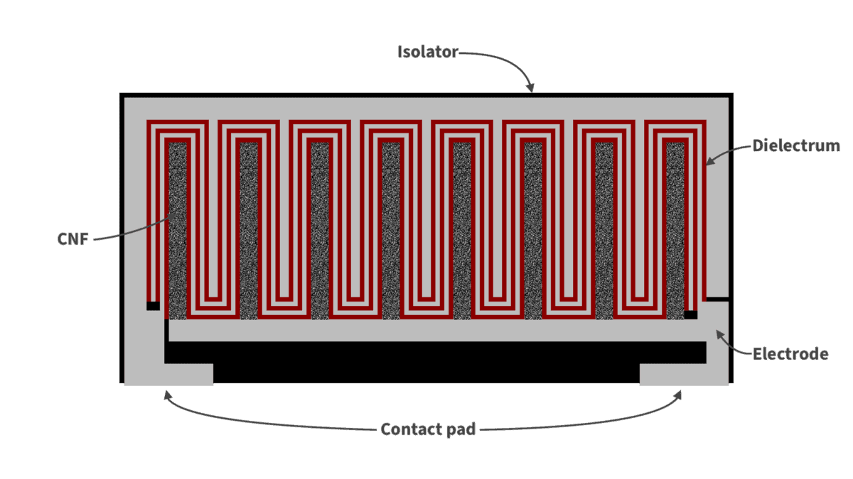
To create a capacitor with a minimal footprint and height, we use carbon nanofibers (CNFs) to multiply the contact area between the two metals and the intermediary dielectric.
Consider a single CNF with a diameter of 10 nm and a length of 5 µm. Its mantle surface is 2,000 times larger than the area it occupies.1 Thus, a forest of such CNFs would multiply the surface, but not by as much as 2,000. We can’t cover the entire original surface with CNFs; there must be space between them to allow access to the contact surface. But if the forest of CNFs covers about half the surface, then the surface multiplication would be in the range of 1,000 times.
CNF has many metallic properties, including being a good conductor of current. Therefore a metal plate covered to fifty percent by CNFs is a single electrode with a surface area about 1,000 times larger than the area of the metal plate itself. By coating this electrode with a uniformly thick layer of a dielectric and then coating this in turn with a metal, a MIM capacitor is obtained. Of course, the dielectric should have a high relative permittivity to maximize the capacitance.
Since the CNF has a length much larger than the diameter, we can neglect what happens to the electric field near the base and top of each CNF. Essentially it will be a uniform field, just as in a parallel plate capacitor.
Since the capacitance of a parallel plate capacitor is directly proportional to the surface area, we conclude that CNFs have increased the capacitance density by 1,000 times.
But it doesn’t end there. If the second layer of metal is made uniformly thick, both sides of it will have the same shape as the first electrode. So by coating it with another layer of dielectric and then coating this in turn with a metal, another MIM capacitor is obtained. It will have the same capacity as the first. And by electrically connecting the first and the third metal layer, we achieve a parallel connection, which doubles the capacitance. This can be repeated as long as desired and there is space between the carbon nanofibers. The last layer of metal does not need to be uniformly thick but can fill in any remaining spaces between the carbon nanofibers.
The figure below shows a discrete CNF-MIM capacitor with three CNF-shaped capacitors connected in parallel. Using the same assumptions about diameter, length, and density as above, this capacitor has 3,000 times the capacitance possible with a parallel plate capacitor in the same location.
Your data will be handled in compliance with our privacy policy.
IR Blog Posts

January 9, 2025
Modern electronics demand increasingly compact and powerful capacitors, and the race for miniaturization has reached a critical juncture. While both Deep Trench Capacitors (DTC) and Carbon Nanofiber Metal-Insulator-Metal (CNF-MIM) capacitors are being developed for advanced applications requiring smaller size and higher capacitance density than conventional surface-mounted capacitors, DTC pushes the boundaries of what’s achievable with subtractive manufacturing, but is hitting fundamental physical limits. In contrast, Smoltek’s innovative CNF-MIM technology offers a revolutionary path forward, unrestricted by these constraints.
IR Blog Posts

September 5, 2024
Smoltek’s focus on qualified research places it firmly in the Explorer quadrant of the R&D Evaluation Matrix, a model for assessing a company’s research and development strategy. Discover why this matters to investors and how Smoltek translates groundbreaking research into valuable business opportunities.
IR Blog Posts

October 1, 2024
Smoltek Semi has developed a new material for use in CNF-MIM capacitors. The new material increases capacitance by more than three times and reduces leakage current by 50 percent. In this article, we examine what this means and why it is good for shareholders and investors.
IR Blog Posts

February 27, 2025
In an age where environmental sustainability is of utter importance, it is crucial to find innovative solutions to reduce energy consumption and minimize our carbon footprint. One such solution is found in capacitors. These unassuming electronic components not only play an important role in various systems, but also offer significant environmental benefits. Albeit very small – if counted one by one.
IR Blog Posts

October 11, 2024
Our innovative “zapping” method drastically reduces development time and costs, enabling us to advance CNF-MIM technology faster and making Smoltek Semi’s technology even more attractive to potential buyers. Read on to see how this new process strengthens our position and shortens our path to market.
IR Blog Posts

June 16, 2025
Smoltek Semi joins an elite club of companies achieving 1 µF/mm² capacitance density, but stands alone in reaching this milestone with an ultra-thin profile. This breakthrough unlocks the under-chip real estate that represents the holy grail of capacitor placement in modern electronics.