Sign up for our newsletter!

Subscribe form (en)

No spam. Simply good reading. Get your free subscription to Smoltek Newsletter infrequently delivered straight to your inbox.

Your data will be handled in compliance with our privacy policy.
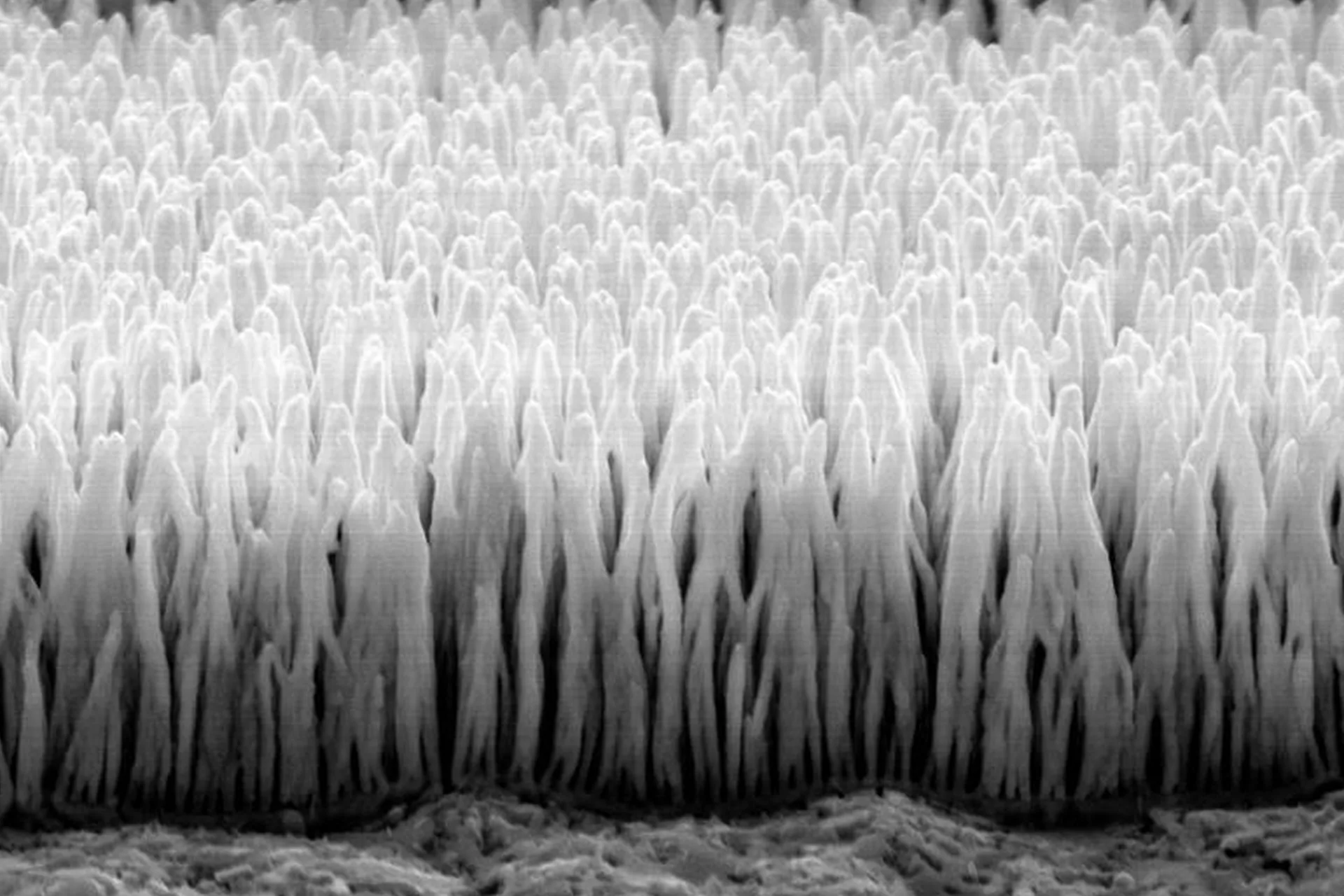
cnf

Carbon nanotechnology

Smoltek’s pat­ent-pro­tec­ted tech­no­logy plat­form enables con­trolled growth of pre­cisely loc­al­ized and defined nano­struc­tures, as indi­vidu­al fibers or clusters, in pre­defined pat­terns or films. This is done in a through cata­lyt­ic growth in a vacu­um cham­ber using gas and cata­lysts. Mater­i­als and pro­cess con­di­tions are com­pat­ible with indus­tri­al requirements.

We have developed unique growth recipes using which we can grow car­bon nano­struc­tures at exact pos­i­tions with exact required prop­er­ties. This is our core tech­no­logy, and it goes by the name Smol­GROW™. Part­ners can license our tech­no­logy to accom­plish solu­tions tailored to their unique needs and requirements.
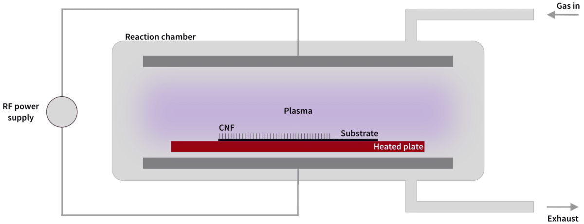
Stronger than steel

Car­bon nan­ofiber is a super mater­i­al. It is stronger, more elast­ic, and light­er than steel. It con­ducts heat and elec­tri­city bet­ter than metals. And it can be used to thou­sand­fold the sur­face of materials. 

A car­bon nan­ofiber (CNF) is a mater­i­al entirely made of car­bon so thin that its dia­met­er is meas­ured in nano­met­ers (nm). Its length is many times longer than its dia­met­er. CNFs have dia­met­ers in the range of 5–500 nm and lengths in the range of 1–200 micro­met­ers (µm).

A nano­met­er (1 nm) is one-thou­sandth of a micro­met­er (0.001 µm). That’s so tiny that only three free car­bon atoms fit on a straight line of that length.1 To get an idea of how extremely small that is, let’s ima­gine a strand of human hair. If you split it length­wise, then split the two halves again, and then repeat this over and over again until you have 70,000 strains from that single strand, each of them is about 1 nm thick.2

Scan­ning elec­tron micro­scope image of a “forest” of car­bon nanofibers.

CNFs are really super strong

Car­bon nan­ofibers are ten times stronger than the strongest steel in the world (mar­aging steel) and up to a hun­dred times stronger than ordin­ary steel.

The tensile strength of car­bon nan­ofibers is a mind-bog­gling 30 giga­pas­cals (GPa).

Sup­pose you have a round bar with a dia­met­er of 1 cm and the same tensile strength as car­bon nan­ofibers. Let’s assume you some­how man­age to hang a mid-size car from its end. Then you add anoth­er, and yet anoth­er, and so on until the round bar breaks. Can you guess how many cars were hanging from the round bar before break­ing? Two hun­dred! That’s how strong car­bon nan­ofibers are.

There­fore, car­bon nan­ofiber is an excel­lent build­ing block at the micro­scop­ic level. It can be used as a sup­port or rein­force­ment bar (“rebar”) for mater­i­als that become brittle at small sizes. They can also be used as tiny spacers between lay­ers of mater­i­als. Or as needles that make micro­scop­ic holes in membranes.

Stiff as a board

If you were going to bend a car­bon nan­ofiber, you’d bet­ter think again. It requires four times more force to bend or stretch car­bon nan­ofibers than steel. And that stub­born little straw would return to its ori­gin­al shape as soon as you let it go. Like a rub­ber band.

The Young’s mod­u­lus (describes the prop­erty of a mater­i­al that tells us how eas­ily it can stretch and deform) of car­bon nan­ofibers var­ies between 80 and 800 GPa.

A lightweight contender

Although a car­bon nan­ofiber is much stronger than steel, it weighs only a quarter of steel. The dens­ity of car­bon nan­ofiber is between 1.3 and 2 g/​cm3.

Ima­gine a steel cube with sides 10 cm long and a car­bon nan­ofiber cube of the same size. If you put them on sep­ar­ate scales, the one with the steel cube will read 8 kg, while the one with the car­bon fiber cube will read less than 2 kg.

Excellent heat conductor

Sil­ver and cop­per are the best heat-con­duct­ive metals. Yet they take a beat­ing com­pared to car­bon nan­ofibers, which can be made to con­duct heat more than sev­en times better.

The thermal con­duct­iv­ity of car­bon nan­ofibers var­ies between 20 and 3,000 Watts per meter Kelvin (W/​mK), depend­ing on how they are manufactured.

That excel­lent heat con­duct­iv­ity can be used to solve one of the biggest prob­lems as more and more tran­sist­ors are crammed onto a chip: Heat dis­sip­a­tion. A chip can become madly hot, short­en­ing its lifespan and increas­ing the risk of fail­ure. But the heat can effect­ively be dis­sip­ated by car­bon nan­ofibers between the chip and the cap­sule enclos­ing it.

Surface multiplier

An excit­ing applic­a­tion for car­bon nano­struc­tures is as sur­face coat­ings to increase the con­tact area. Grow­ing car­bon nano­struc­tures dir­ectly on a sur­face can increase the con­tact area tens of thou­sands of times.

Ima­gine a square sur­face with a width and a height of one mil­li­meter. It can eas­ily hold 100,000 rows and as many columns of car­bon nan­otubes being 5 nano­met­ers in dia­met­er and 50 micro­met­ers in length. The sur­face area of those car­bon nan­otubes increases the total sur­face area 7 855 times. In oth­er words, car­bon nan­otubes can eas­ily shrink an area of 88×88 mil­li­meters to just 1×1 millimeters.

Increas­ing the sur­face area many thou­sand folds is bene­fi­cial in vari­ous applic­a­tions. One example is car­bon nan­ofibers coated with titani­um on the sur­face of a titani­um implant. The implant’s sur­face area will increase, mak­ing it easi­er to join the bone. Anoth­er example is the mini­atur­iz­a­tion of capacitors.

Carbon nanofibers at the atomic level

What makes CNF so unique is how the car­bon atoms are arranged. To under­stand how we must first review some basic atom­ic theories.

Bohr’s clas­sic­al mod­el of an atom describes it as a nuc­le­us sur­roun­ded by shells of elec­trons. Each shell has room for a fixed num­ber of elec­trons. The inner­most shell has two loc­a­tions. The fol­low­ing shell has room for eight elec­trons. And so on.

In most cases, the shells fill up from the inside out. When a shell is com­plete, it is said to be closed. If it’s not com­plete, it is, of course, called open.

Elec­trons in the out­er­most shell are called valence elec­trons. Only noble gases have valence elec­trons in a closed shell. They are super stable. All oth­er sub­stances have valence elec­trons in an open shell, which can do crazy things.

For example, a valence elec­tron in an open shell can attract anoth­er atom and, in exchange for it, also serve as the valence elec­tron for the oth­er atom. In this way, the two atoms will share an elec­tron. This cre­ates a bond between the two atoms. This type of bond, where the atoms share one or more elec­trons equally, is called a cova­lent bond.

A car­bon atom has six elec­trons: Two are in the inner­most elec­tron shell (which is there­fore closed), and four are in the shell out­side (which is there­fore open). So the car­bon atom has four valence elec­trons but “needs” four more to close the out­er shell. There­fore, free car­bon atoms do not become long-lived; they soon find oth­er atoms to cre­ate cova­lent bonds with.

A car­bon atom can fill the out­er shell with a valence elec­tron, form­ing a cova­lent bond with anoth­er car­bon atom. These, in turn, can do the same. Sup­pose this is repeated over and over again. In that case, we get a molecule made up of car­bon atom after car­bon atom. The prop­er­ties of these car­bon atoms depend on how they arrange themselves.

Allo­tropy is the phe­nomen­on of cer­tain ele­ments that can exist in dif­fer­ent forms called allo­tropes. Car­bon has many allotropes.

A three-dimen­sion­al array of car­bon atoms, where each bond has the same angle as its neigh­bors, is called a dia­mond.

Car­bon atoms that form hexagon­al rings, where adja­cent rings share sides and are in the same plane, are called graphene. It looks like a sheet of chick­en wire where the knots are car­bon atoms, and the threads between them are cova­lent bonds.

Graph­ite is lay­ers upon lay­ers of graphene. The lay­ers are held togeth­er by quantum dynam­ic inter­ac­tions between atoms in adja­cent lay­ers called van der Waals force.

Car­bon atoms that form five‑, six- or sev­en-sided rings, where adja­cent rings share sides but are not in the same plane, are called fullerene. These occur in many dif­fer­ent forms, many of which have their own names. In a sense, graphene is just a spe­cial case.

A fullerene that looks like a tube pos­sibly closed at the end is said to be a single-wall car­bon nan­otube (SWCNT) or car­bon nan­otube (CNT) for short. A multi-wall car­bon nan­otube (MWCNT) con­sists of one SWCNT enclos­ing anoth­er SWCNT, pos­sibly enclos­ing a third SWCNT, and so on. The nes­ted SWCNTs are “glued” to each oth­er by the van der Waals force.

Finally, we have arrived at the car­bon nan­ofiber (CNF), which can be seen as a “mod­i­fied MWCNT” where each tube is tightened at one end so that they take the shape of a plate, cup, or cone before they are stacked one inside the other.

How are CNFs manufactured?

Com­mer­cial fab­ric­a­tion of car­bon nan­ofibers is often done with Cata­lyt­ic Chem­ic­al Vapor Depos­ition (CCVD, or simply CVD). The basic idea is to apply so much energy to a car­bon-based gas, in the form of heat­ing or light­ning dis­charges, that the valence elec­trons are torn loose, releas­ing car­bon ions that can depos­it on sur­faces pre­pared with cata­lyt­ic metal.

Smol­tek has developed a pat­en­ted solu­tion to extremely pre­cise con­trol where the released car­bon atoms settle and how they are formed into car­bon nan­ofibers. This gives us a unique oppor­tun­ity to tail­or car­bon nan­ofibers with desired prop­er­ties. We have also developed the tech­no­logy to use com­par­at­ively low tem­per­at­ures (375 °C), which allows our man­u­fac­tur­ing tech­nique to be used in pro­duc­tion lines in the semi­con­duct­or industry.

The fol­low­ing is a sim­pli­fied descrip­tion of our man­u­fac­tur­ing pro­cess, which we call SmolGROW™:

  1. The sub­strate on which the car­bon nan­ofibers will grow, e.g., sil­ic­on wafer, is pre­pared by depos­it­ing vari­ous mater­i­als that form an under­lay­er on which the car­bon nan­ofibers will grow.
  2. A cata­lyst is depos­ited as dots or pads where car­bon nan­ofibers will grow on top of the under­lay­er. These facil­it­ate a con­trolled growth of indi­vidu­al nano­struc­tures in pre­cise locations.
  3. The sub­strate is put into a react­or cham­ber, which is her­met­ic­ally sealed and emp­tied of air, mak­ing a vacu­um inside.
A pre­pared sub­strate is placed in the PECVD reac­tion chamber.
  1. A car­bon-based gas is intro­duced into the react­or cham­ber along with oth­er gases that facil­it­ate the reac­tion. Typ­ic­ally, acet­ylene is used to grow the fibers and the ammo­nia to clear excess deposition.
  2. Inside the cham­ber, a huge dif­fer­ence in elec­tric­al voltage cre­ates an arc of light (elec­tric­al dis­charge). This heats the gas so that elec­trons are sep­ar­ated from the nuc­lei and can move freely. The res­ult is a soup, called plasma, of elec­trons and ions. The dis­charges are repeated sev­er­al times per second to main­tain the plasma. One of the cru­cial prop­er­ties of plasma is that the elec­trons have an energy equi­val­ent to sev­er­al thou­sand degrees Celsi­us. At the same time, the rest of the gas is rel­at­ively cool.
  3. The elec­trons’ energy induces the depos­ition of car­bon on the cata­lyt­ic dots and pads, which form a car­bon nano­struc­ture. Smol­tek can cre­ate vari­ous car­bon nano­struc­tures by con­trolling the depos­it, includ­ing car­bon nan­ofibers with desired properties.
  4. When the car­bon nan­ofibers have reached the desired length, the pro­cess is stopped, and the remain­ing gases are ven­ted out of the cham­ber again. We are left with the sub­strate with the car­bon nanofibers.

Smoltek’s tech­no­logy works not only with car­bon nan­ofibers. It is pos­sible to cre­ate oth­er car­bon nano­struc­tures, like car­bon nan­otubes (CNTs), and use mater­i­als oth­er than carbon.

Schem­at­ic dia­gram show­ing how car­bon nan­ofibers (CNFs) are placed for growth in a 
Plasma Enhanced Chem­ic­al Vapor Depos­ition (PEVCD) reac­tion chamber.
  1. If you think of a free car­bon atom as a hard-sphere, its dia­met­er is 0.34 nm. Its van der Waals radi­us is 0,17 nm. ↩︎
  2. The thick­ness of a strand of hair var­ies from 0.017 to 0.18 mm, but the most com­mon is around 0.07 mm. ↩︎

Learn more

Learn more about carbon nanotechnology from the articles below, or contact us and let’s have a chat.

Green World

Carbon nanofibers in the hydrogen industry

With our carbon nanofibers (CNFs) fabrication technology, we develop advanced materials engineering solutions for use in water electrolysis and fuel cells for the hydrogen industry.

Adobestock 165717610

Carbon nanofibers in the semiconductor industry

With our carbon nanofibers (CNFs) fabrication technology, we develop advanced packing solutions and ultra-miniaturized capacitors for use in the semiconductor industry.

Cultivation Of Precisely Placed Carbon Nanofibres

What is a carbon nanofiber (CNF)?

Carbon nanofibers is a supermaterial. It is stronger, more elastic, and lighter than steel. It conducts heat and electricity better than metals. And it can be used to thousandfold the surface of materials. Let’s take a closer look at these tiny fellows.

Adobestock 250253567

Miniaturized capacitors with carbon nanofibers

Smoltek has developed the world’s thinnest discrete capacitor. You have to stack ten of them on top of each other to reach the same height as today’s industry-standard when it comes to surface-mounted capacitors. The most amazing thing about this microscopic capacitor is its performance. One square millimeter has a capacitance of a whopping 650 nanofarads (650 nF/mm2). Read on for more details.

H2

Carbon nanofibers in hydrogen electrolysis and fuel cells

Carbon nanofibers in hydrogen electrolysis & fuel cells Hydrogen has emerged as a key to store renewable energy and making heavy industry carbon-free. Two application areas of immediate vital importance. The core technologies that make this possible are hydrogen electrolysis and fuel cells. Electrolysis converts electricity into hydrogen, while fuel cells convert the hydrogen back to electricity.