Sign up for our newsletter!
Your data will be handled in compliance with our privacy policy.
Your data will be handled in compliance with our privacy policy.

Smoltek has produced a quarter million capacitors (without carbon nanofiber) and has begun producing a new batch (with carbon nanofiber). This is huge because it shows that our high-volume manufacturing process works. It is intended to be used to produce engineering samples. You could read about this in a press release. In this article, we unpack what this means.
Thomas Barregren • October 12, 2023
When writing press releases, words are weighed on a golden scale. A lot of information has to be squeezed into a small space. As a public company, weighing the words to minimize the risk of misunderstandings is even more critical. This is how it should be. As a shareholder or investor, you expect no less.
But there are two sides to every coin.
The disadvantage of these information dense press releases is that the big picture may be lost. It’s easy to miss the forest for the trees.
Therefore, from time to time, we will pick up recently published press releases in this blog and unpack their implications.
Let’s start with “Smoltek has developed a process for production of engineering samples in high volumes which are expected to be available before the end of Q4 2023”.
If you read the press release carefully, you will find five news items:
We will go through each of these news items and discuss their significance. Let’s begin.
Our business division for the semiconductor industry, Smoltek Semi, has for some time had a strong focus on commercializing its capacitor that use carbon nanofibers to deliver unmatched capacitance per unit area and unit height. We call them CNF-MIM capacitors because they use carbon nanofibers (CNF) to create highly tight-packed metal-insulation-metal (MIM) capacitors.
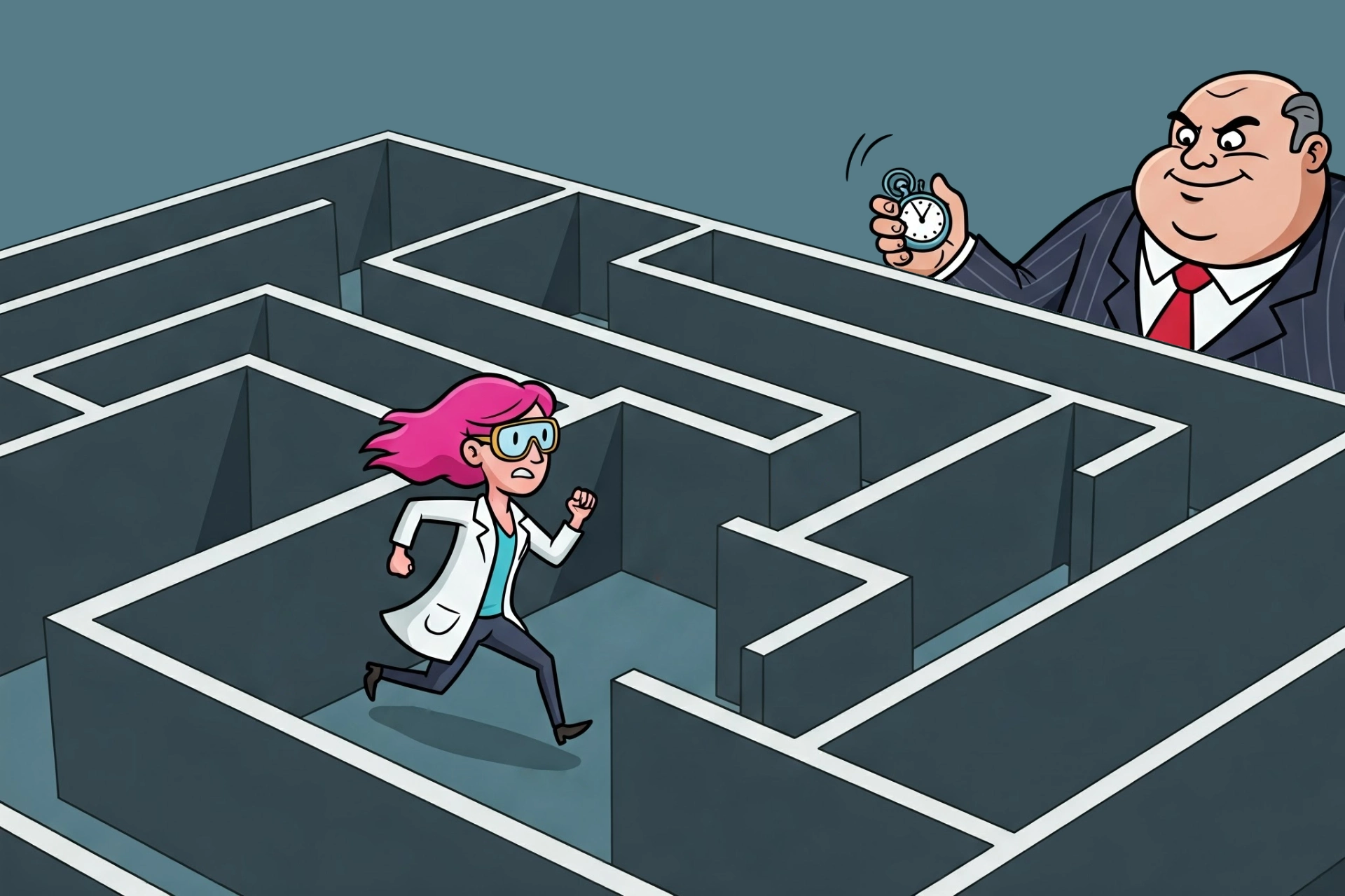
The road from the first capacitor to mass production is long, but we are approaching the goal as planned. We are now in the midst of an essential step: producing engineering samples.
This step is significant for two reasons.
First of all, it is necessary to offer engineering samples because the big electronics companies don’t buy a pig in a poke; they require samples to test. Just like you test drive a new car model before you buy it, they want to test drive new electronic components before using them in mass production. So, it is necessary to offer engineering samples to sell.
This brings us to the second reason this step is significant: It enables customer interaction. Next year, we will start sales by convincing electronics manufacturers to choose our capacitor technology for their designs. If everything goes according to plan, we will mass-produce CNF-MIM capacitors before 2027.
We have been working for some time to take the manufacture of CNF-MIM from the lab to the industry. That is not a trivial task.
It’s one thing to produce single CNF-MIM capacitors in the lab and quite another to mass manufacture them on a large scale. In the lab, we can do pretty much what we want. But for high-volume production, we must adapt the process to industrial standards, use readily available tools and materials, and ensure the fastest, easiest, and smoothest process possible.
We have come a long way in doing so. We have now implemented a process with our partners that enables us to produce high-volume engineering samples.
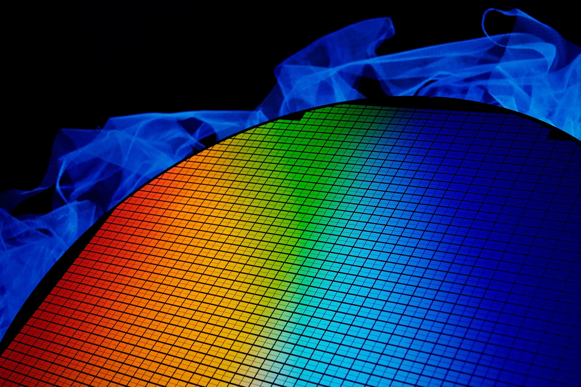
An example of adaptation we have made going from the lab to the industry is the introduction of 8‑inch diameter wafers.
A wafer is a circular silicon disc usually used to make integrated circuits, known as chips. Wafers exist in different sizes, from 2 inches in diameter to 12 inches. The choice of size is a compromise between producing many chips in a single batch and the risk of losing many chips due to manufacturing errors.
We have so far worked with 4- and 6‑inch wafers. But we have adapted our process to 8 inches, the industry’s most common size in our new high-volume manufacturing machine. We have also rebuilt our current machine so that an 8‑inch wafer can physically fit in, even though the effective area is equivalent to a 6‑inch wafer.
Another example of adaptation is that we mainly work with tools that are commonly used in industry.
We have produced a first batch of ten wafers with 27,000 capacitors each. That is more than a quarter of a million capacitors.
The manufactured capacitors are metal-insulation-metal (MIM) without carbon nanofiber (CNF). Thus, they are MIM capacitors but not CNF-MIM capacitors.
So why did we do a batch without carbon nanofibers?
Producing MIM capacitors on semiconductors is a highly complex task. It requires several steps by different partners specialized in their respective fields. We wanted to validate that our partners could produce capacitors with consistent properties and good quality in a stable and repeatable way. So, by eliminating the carbon nanofibers from the equation, we were able to validate that the process steps our partners make meet our high standards. We are delighted with the results.
We have already started production of a new trial batch that is identical in all respects to the first one, except that we are now adding carbon nanofibers. We expect to finish this second batch before the end of this year.
When we receive the new batch, we will together with our partner YAGEO test the electrical properties. We are ready to start producing and shipping engineering samples if they meet our high expectations.
Did this article give you a better understanding of the meaning of the press release? Visit our IR page on LinkedIn and tell us what you thought of the post. The floor is yours.
Your data will be handled in compliance with our privacy policy.
IR Blog Posts
April 10, 2025
For industrial enterprises, bringing new technologies into existing product lines follows a structured process. Understanding this process is vital for high-tech companies seeking integration partnerships. Here, we explain the systematic journey that governs how industrial enterprises evaluate and adopt innovations, and how high-tech companies can create revenue opportunities at each stage along the way.
IR Blog Posts

October 1, 2024
Smoltek Semi has developed a new material for use in CNF-MIM capacitors. The new material increases capacitance by more than three times and reduces leakage current by 50 percent. In this article, we examine what this means and why it is good for shareholders and investors.
IR Blog Posts

February 27, 2025
In an age where environmental sustainability is of utter importance, it is crucial to find innovative solutions to reduce energy consumption and minimize our carbon footprint. One such solution is found in capacitors. These unassuming electronic components not only play an important role in various systems, but also offer significant environmental benefits. Albeit very small – if counted one by one.
IR Blog Posts

October 11, 2024
Our innovative “zapping” method drastically reduces development time and costs, enabling us to advance CNF-MIM technology faster and making Smoltek Semi’s technology even more attractive to potential buyers. Read on to see how this new process strengthens our position and shortens our path to market.
IR Blog Posts

July 30, 2025
The recently signed technical service agreement between Smoltek Semi and the Industrial Technology Research Institute (ITRI) of Taiwan changes how CNF-MIM capacitors will reach the market. This partnership delivers the validation and manufacturing capabilities needed to transform laboratory breakthroughs into commercial reality.
IR Blog Posts

September 5, 2024
Smoltek’s focus on qualified research places it firmly in the Explorer quadrant of the R&D Evaluation Matrix, a model for assessing a company’s research and development strategy. Discover why this matters to investors and how Smoltek translates groundbreaking research into valuable business opportunities.