Sign up for our newsletter!
Your data will be handled in compliance with our privacy policy.
Your data will be handled in compliance with our privacy policy.

Research

December 28, 2014
Research paper in the proceedings of Semicon Taiwan 2014.
Research
September 25, 2014
Research paper in the proceedings of 2014 IEEE 64th Electronic Components and Technology Conference (ECTC), 2014, pp. 1071–1076.
Research

August 20, 2014
Research article published in EUROSENSORS 2014, the 28th European Conference on Solid-State Transducers.
Research
June 30, 2014
Research paper in the proceedings of MEMSWAVE 2014, La Rochelle, France, 30 June–2 July, 2014.
Research

June 29, 2014
Research paper in the proceedings of Annual World Conference on Carbon (Carbon 2014): Carbon Materials for Ubiquitous and Sustainable Life, Jeju, Korea, 27 June–4 July, 2014.
Research

June 22, 2014
Research paper in the proceedings of 16th European Conference on Composite Materials, ECCM16, Seville, Spain; 22–26 June, 2014.
Research
April 16, 2014
Research paper published in the IPC APEX EXPO Conference Proceedings, March 23–27, 2014.
Research
April 15, 2014
Article published in MEPTEC Report, Volume 18, Issue 1.
Research
May 12, 2013
Research paper in the proceedings of 2nd International Conference on Materials for Energy (EnMat II), Karlsruhe, Germany, 12–16 May, 2013.
Research
July 10, 2011
Research paper in the proceedings of NT11 International Conference on the Science and Application of Nanotubes, University of Cambridge, United Kingdom, July 10–16, 2011.
Patents
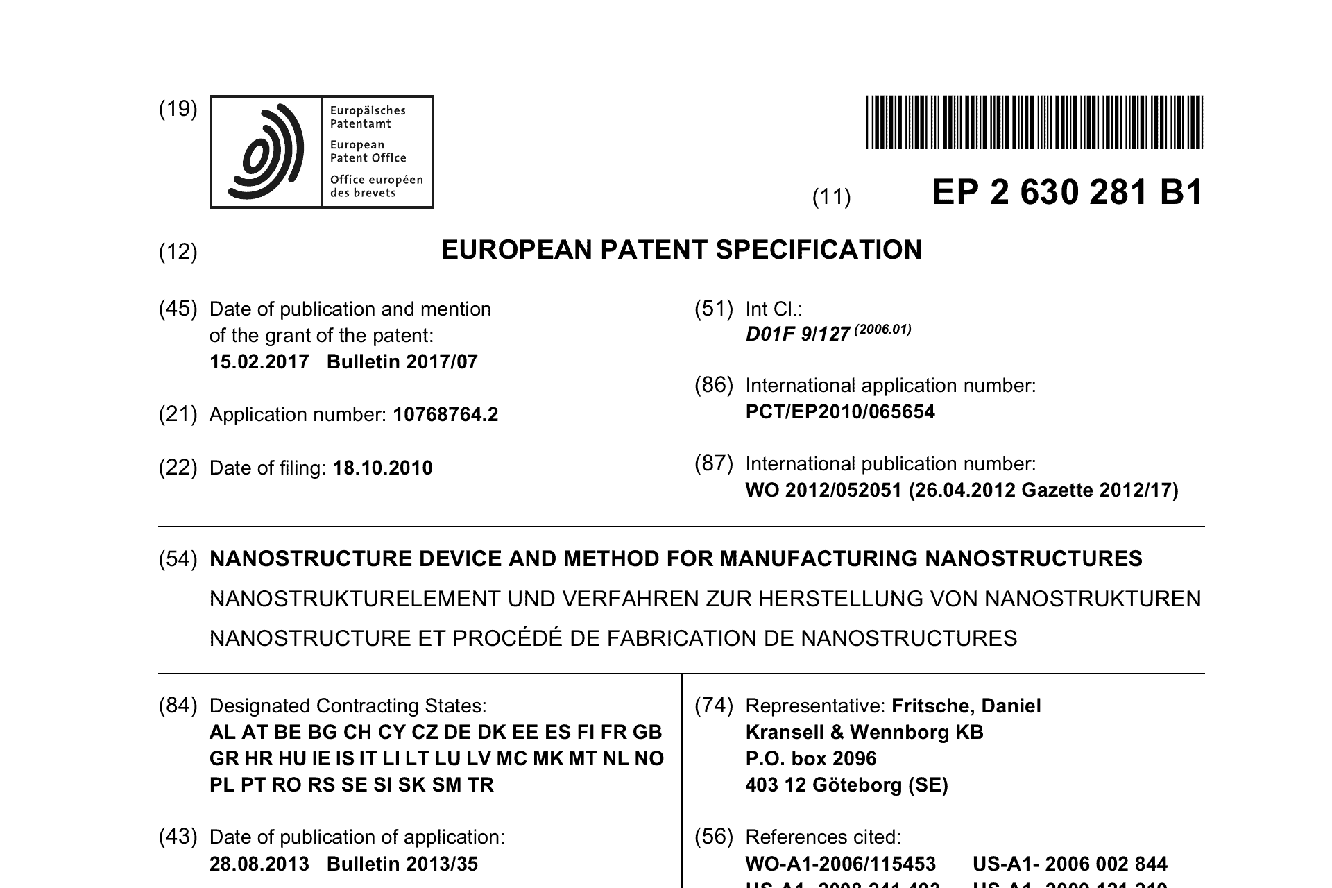
October 18, 2010
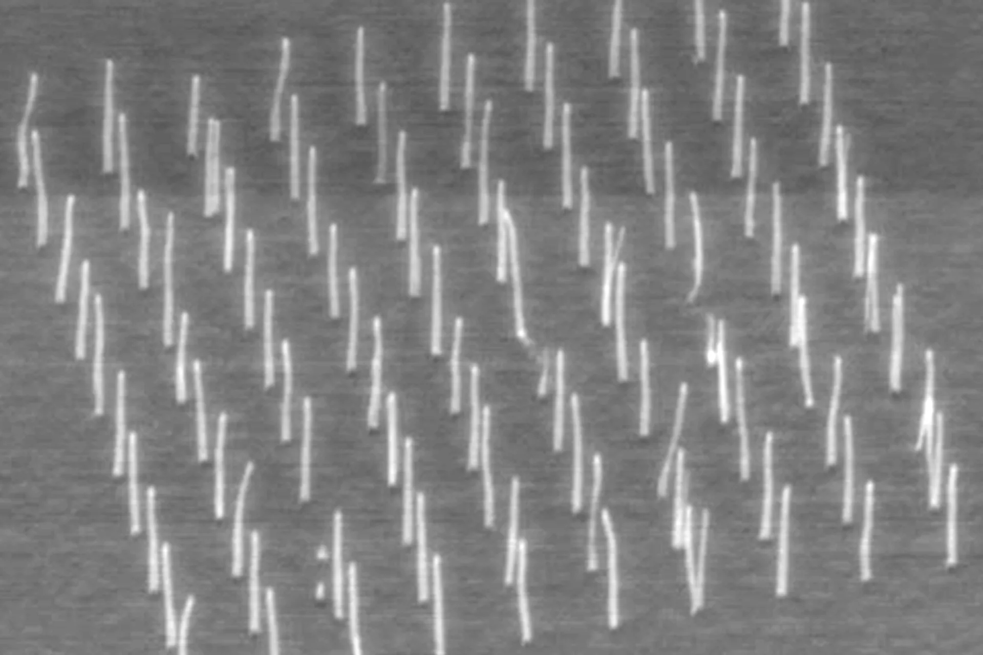
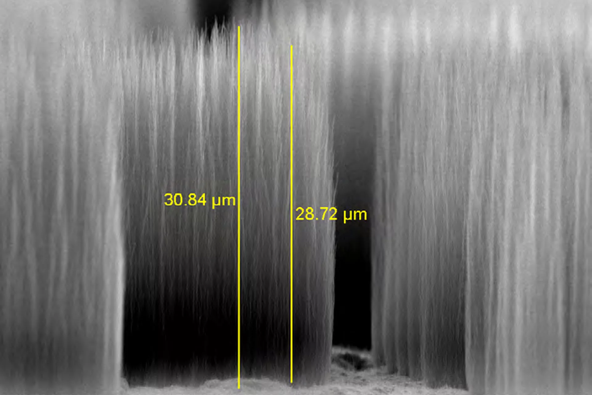
The Catalyst Diffusion family is covering a method for manufacturing a plurality of nanostructures on a substrate.
Research
August 26, 2009
Research paper published in Nanotechnology, 2009, Volume 20, Number 37, pp. 375302–375306.
Patents
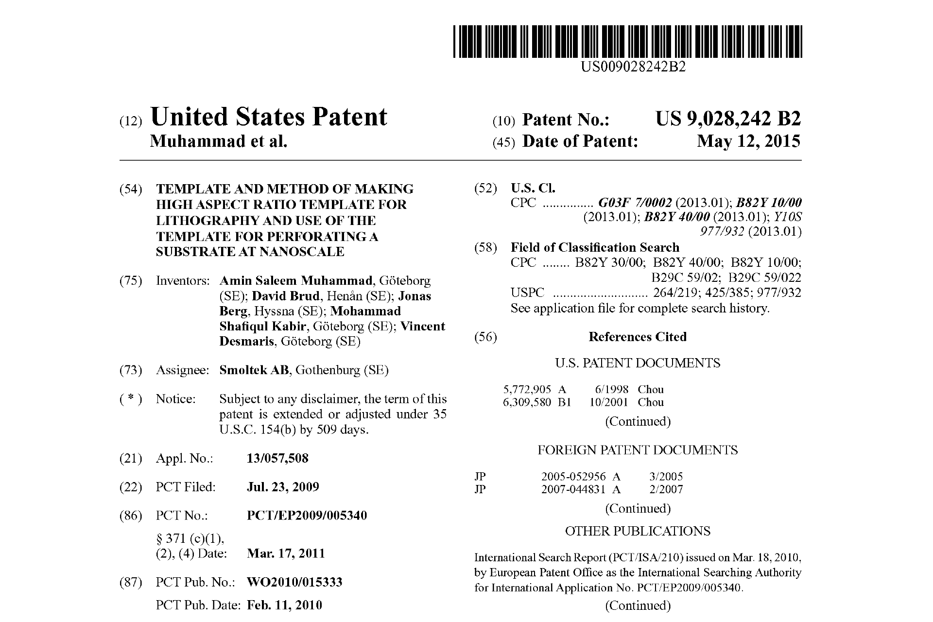
July 23, 2009
The Nano Imprint Lithography family is covering a method of making high aspect ratio template, stamp, and imprinting at nanoscale using nanostructures.
Patents
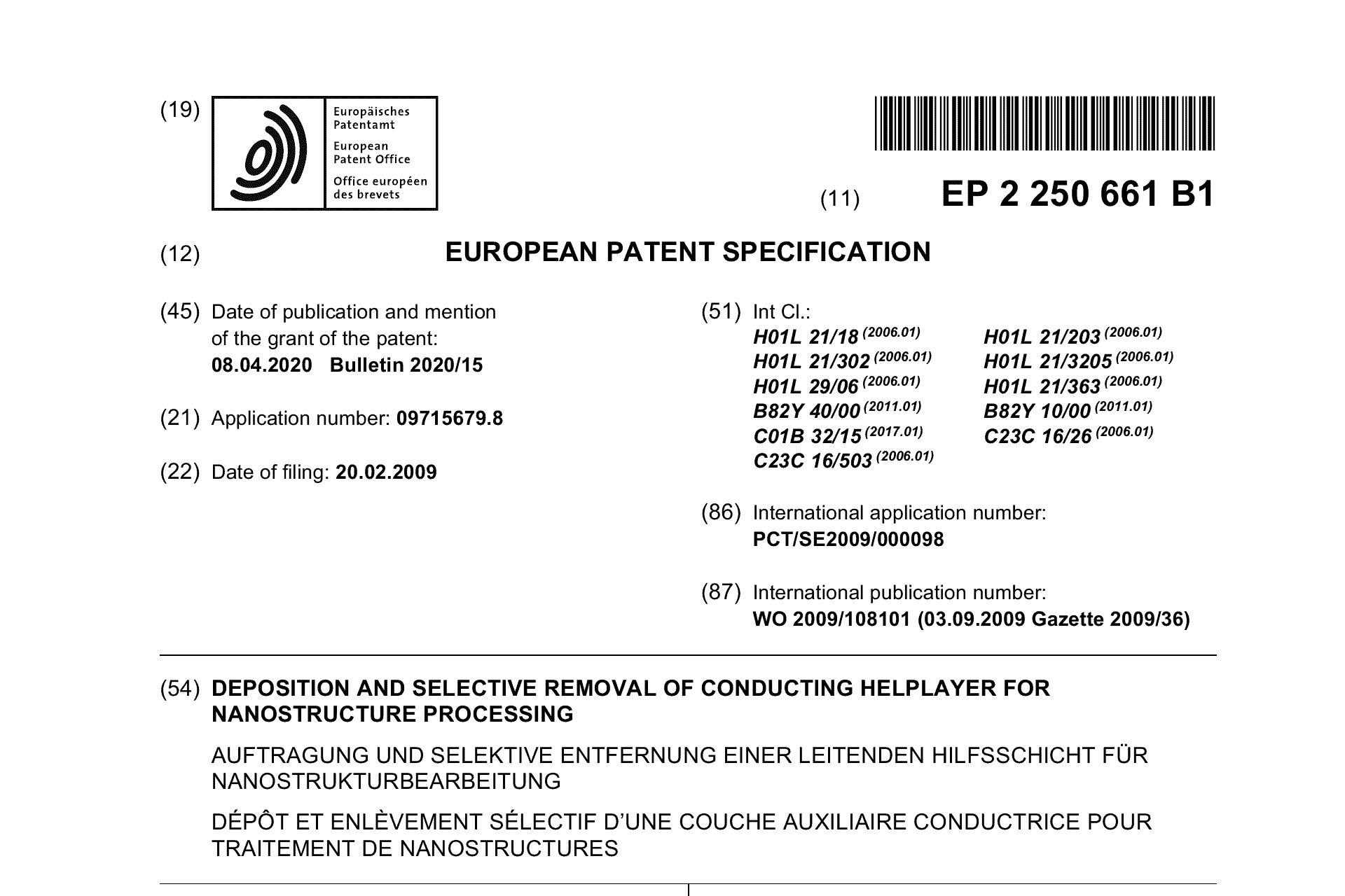
February 20, 2009
The Helplayer family is covering a method to protect the underlaying substrate or materials from being damaged during the nanostructure growth process.
Research
January 1, 2009
Article published in Nanotechweb, 2009.
Patents
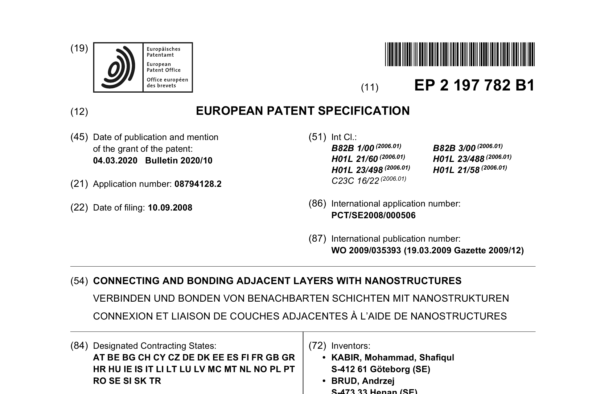
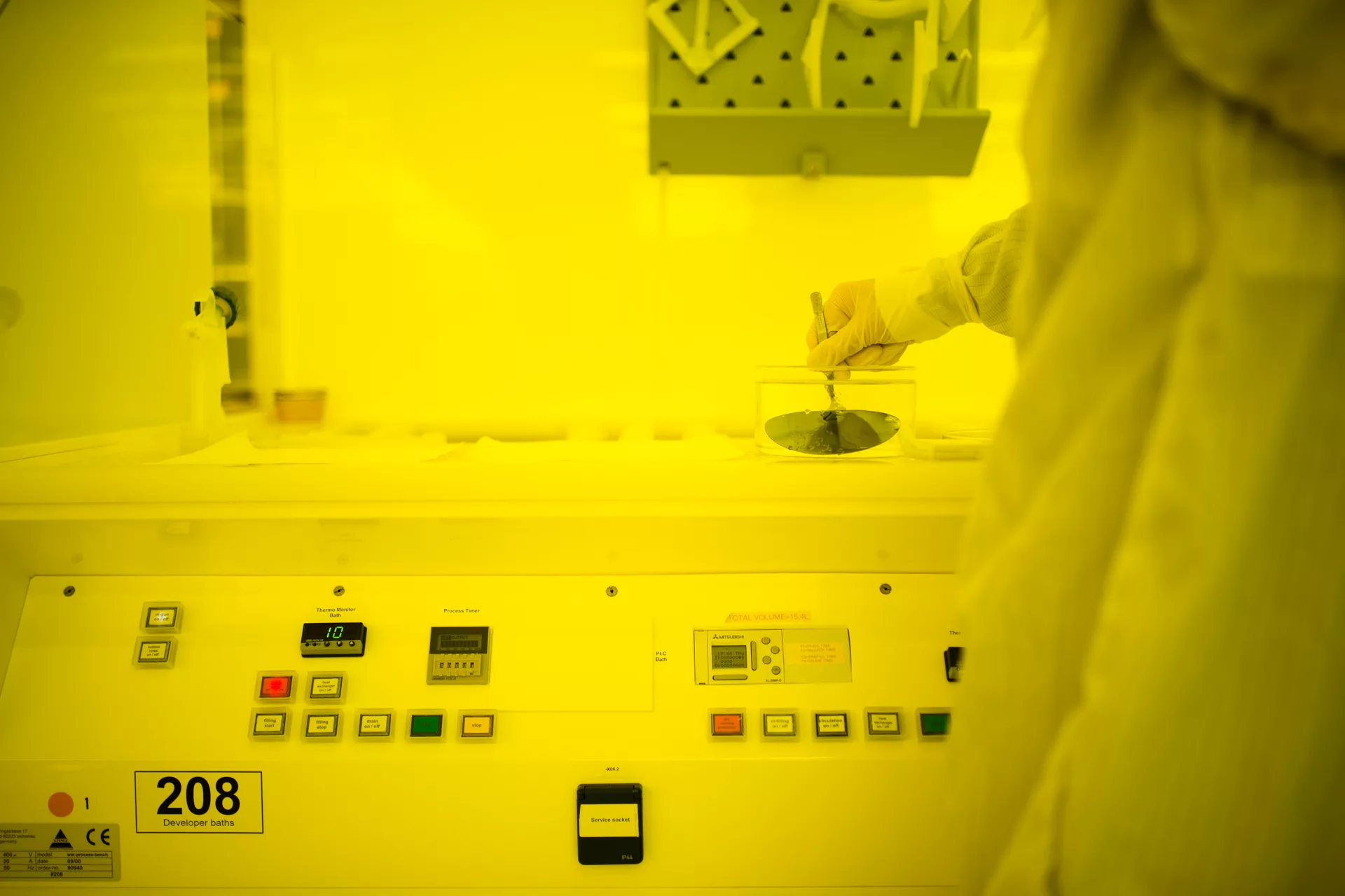
September 10, 2008
The Bumping family is an apparatus connecting and bonding adjacent layers with nanostructures.
Research

July 18, 2008
Research paper published in Nano Letters 2008, Volume 8, Issue 8, pp. 2437–2441, July 18, 2008.
Patents
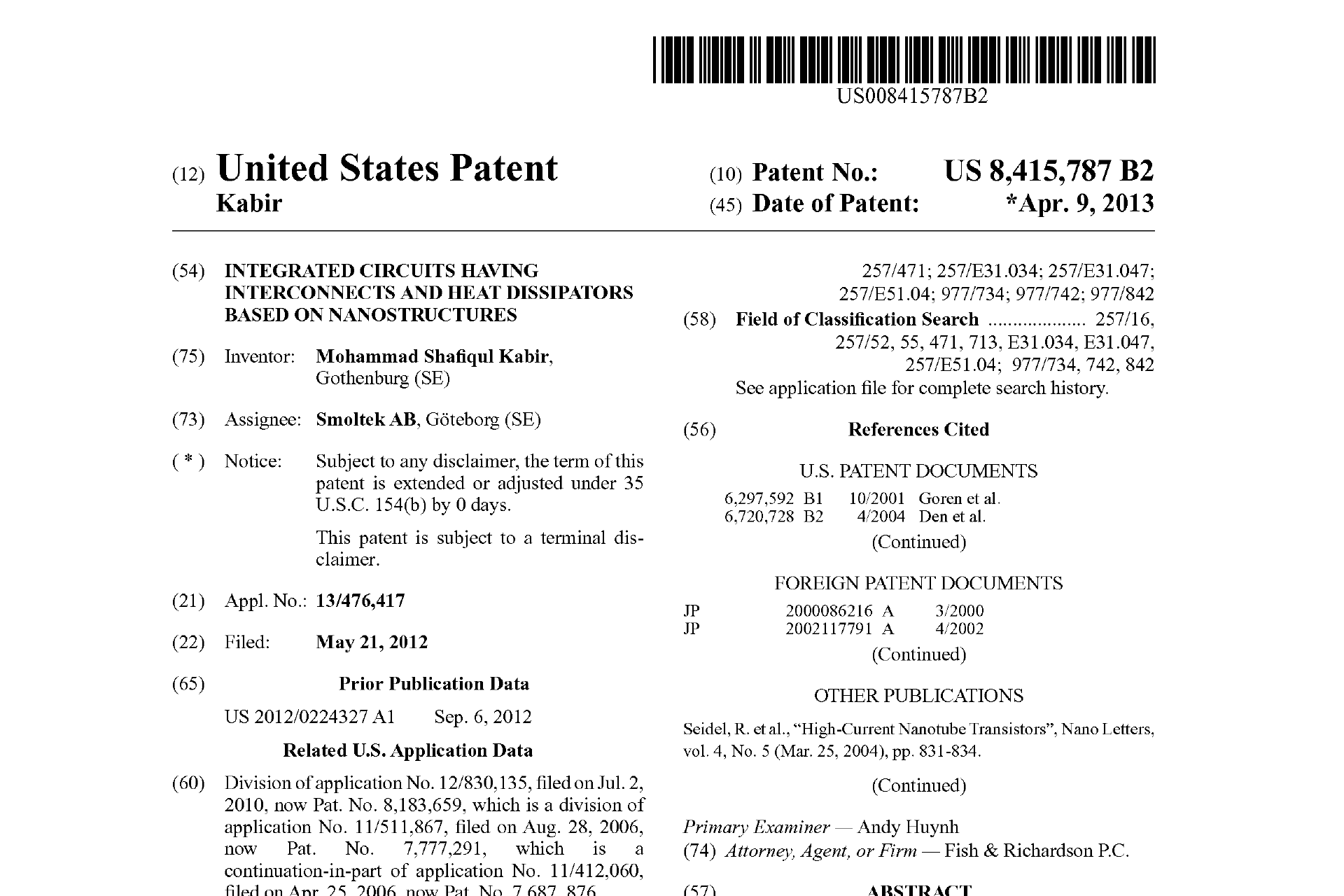
August 28, 2006
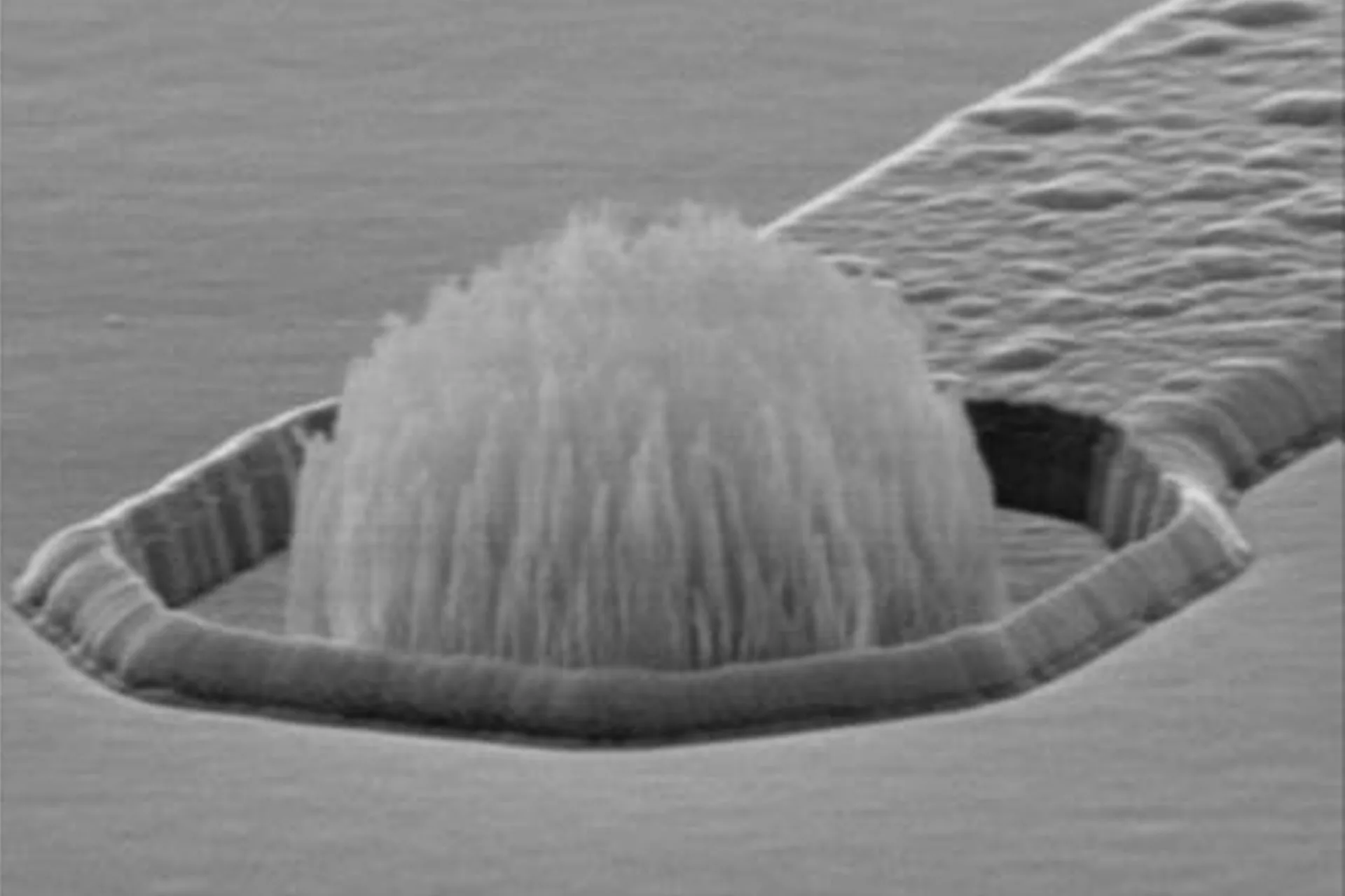
The Interconnects B family is covering how nanostructures can be used as interconnects and/or for dissipating heat from electronic devices.
Patents
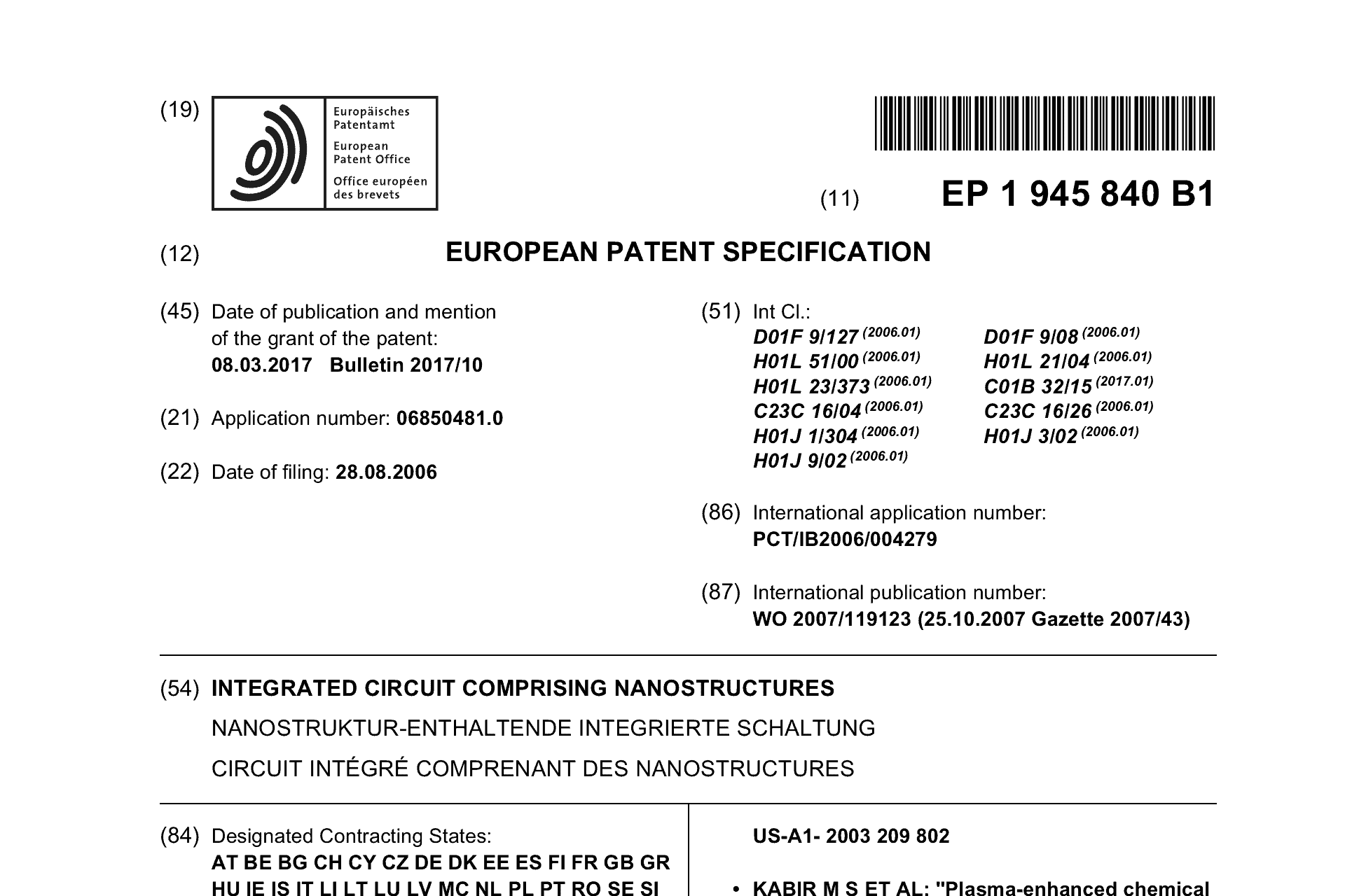
August 28, 2006
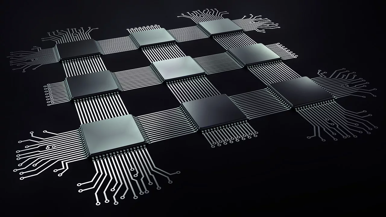
The Nanostructure IC family is covering a method for the manufacture of an integrated circuit comprising nanostructures.
Patents
April 25, 2006
The Interconnects A family is covering a method regarding controlled growth of a nanostructure on a substrate, and electron emission devices based on the same.