Sign up for our newsletter!
Your data will be handled in compliance with our privacy policy.
Your data will be handled in compliance with our privacy policy.

Patents
August 1, 2024
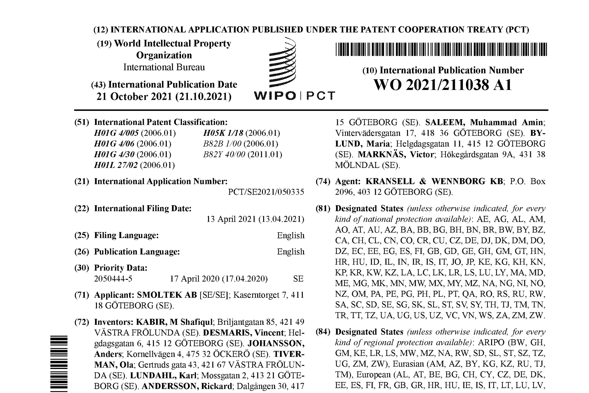
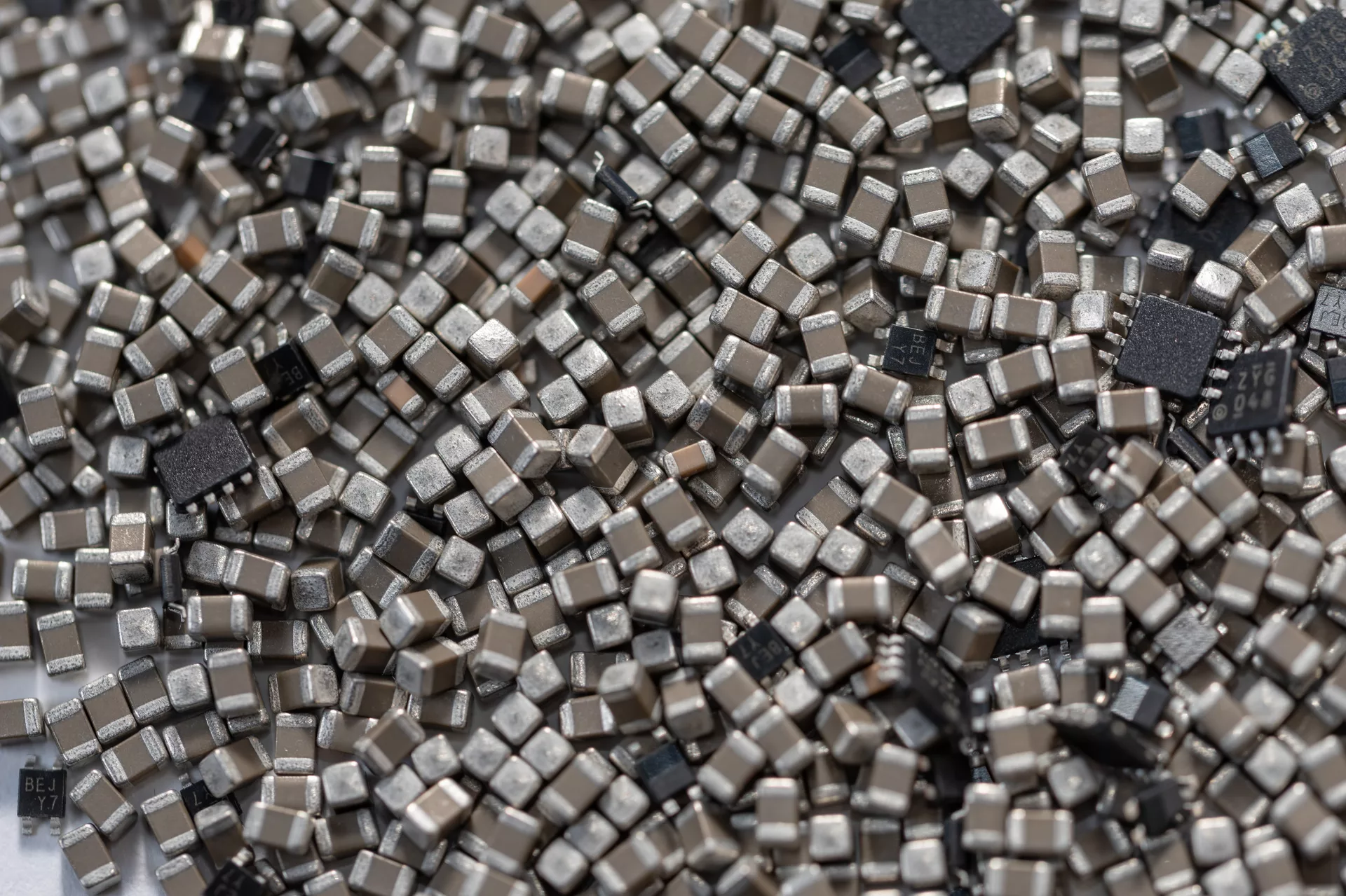
The Multilayer Cap patent family introduces a MIM-capacitor device that can double or triple the capacitance density of Smoltek's CNF-MIM capacitors. The patent details an invention for a layered energy storage device, specifically a capacitor, built using a metal-insulator-metal (MIM) configuration.
News
February 28, 2024
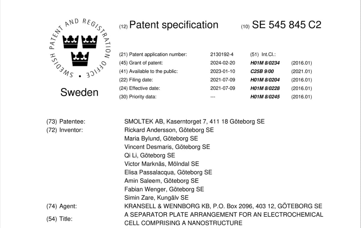
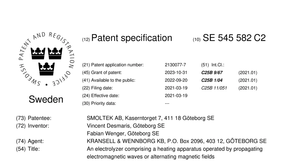
Smoltek has three new patents granted – in three new and separate patent families, all related to how our technology can reduce contact resistance between different layers in electrochemical cells, mainly for use in electrolyzers and fuel cells. These new patents also bring our IP portfolio to comprise 87 granted patents.
Patents
February 27, 2024
The Contact Resistance patent family is covering how to improve a separator plate arrangement for an electrochemical cell by comprising a nanostructure which offers lowered contact resistance between the separator element and the diffusion layer.
News
November 8, 2023
Smoltek is awarded a new patent. This patent is also the first one in a new patent family called Electro Catalyst Heating, which discloses a way of facilitating endothermic electrocatalytic reactions by adding heat in the catalytic structure in the electrolyzer cell. This patent also brings our IP portfolio to comprise 83 granted patents.
Patents
November 8, 2023
The Electro Catalyst Heating family is covering a way of arranging a temperature gradient in the electrolyzer by increasing a temperature of the catalyst structure. The innovation is targeted towards the production of green hydrogen using PEM electrolyzers.
News
August 24, 2023
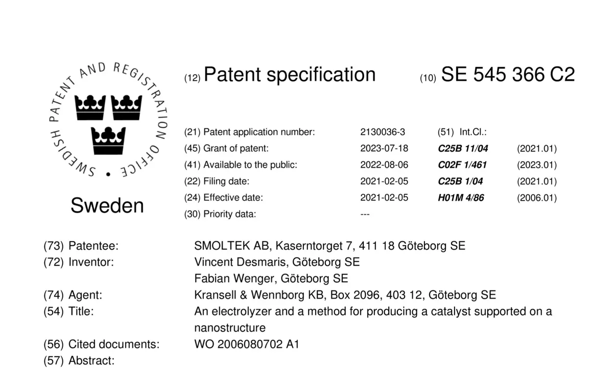
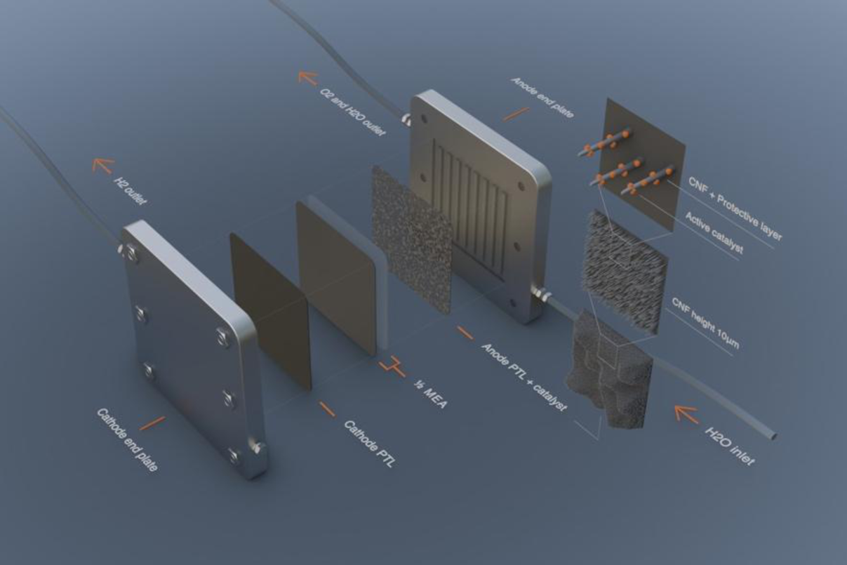
Smoltek is awarded a new patent. The first one in a new patent family called Electro Catalyst Support, which is targeted towards the production of green hydrogen. This innovation discloses how our carbon nanofibers can support the iridium catalyst load in a PEM-electrolyzer in a better way. This patent also brings our IP portfolio to comprise 80 granted patents.
Patents
August 18, 2023
The Electro Catalyst Support family is covering an electrolyzer and a method for producing a catalyst supported on a nanostructure. The innovation is targeted towards the production of green hydrogen and discloses how carbon nanofibers can support the iridium catalyst load in a PEM-electrolyzer in a better way.
Patents
June 13, 2023
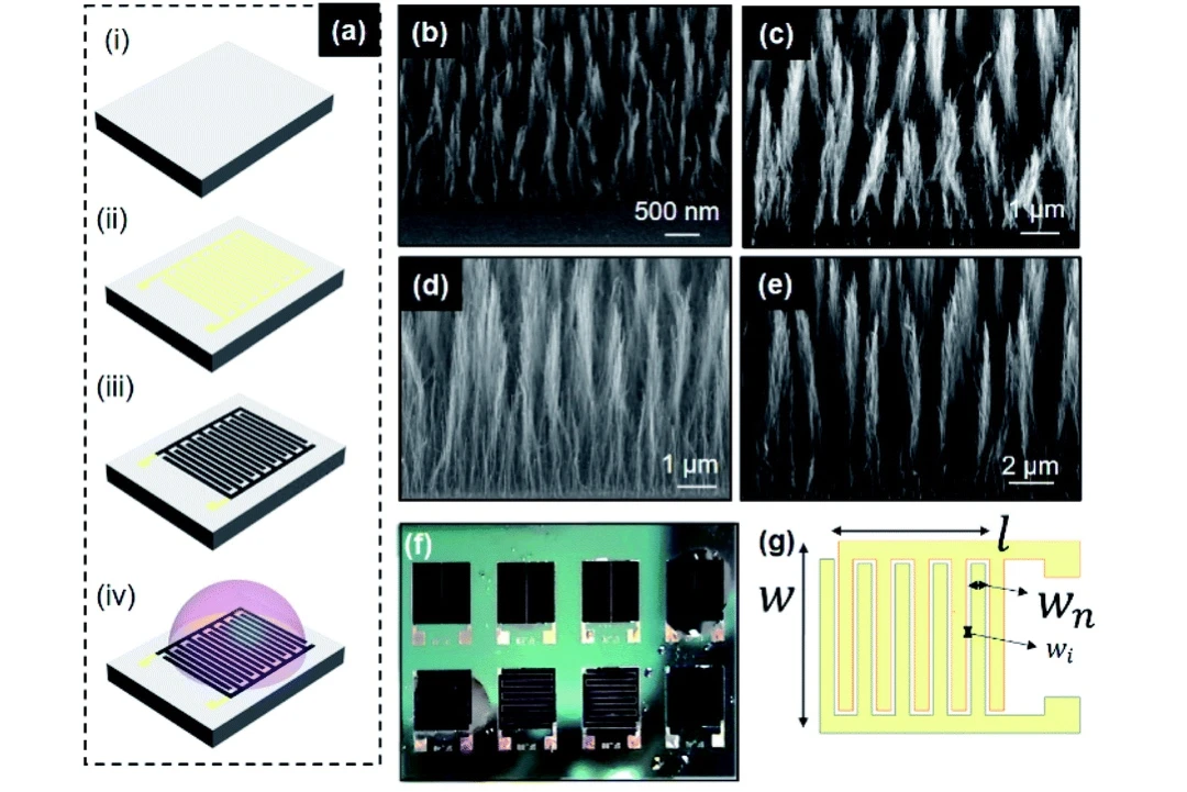
The Discrete CNF-MIM patent family is covering a method for manufacturing of discrete capacitor components based on our CNF-MIM technology. The innovation exploits the extra-ordinary surface to volume ratio provided by carbon nanofibers to create a MIM capacitor with unparalleled high capacitance density.
Research
August 20, 2022
Research paper published in the proceedings at ICE 2021, the 3rd International Conference on Electrolysis June 20 – 23, 2022 Golden, Colorado USA.
Research
October 2, 2021
Research paper published in the proceedings at the 3rd PCNS 7-10th September 2021, Milano, Italy as paper No.5.3. and voted by attendees as: BEST PAPER AWARD.
Research
August 10, 2021
Research paper published in the proceedings of 2021 IEEE 71st Electronic Components and Technology Conference (ECTC), 2021, pp. 2229-2234.
Research
August 10, 2021
Research paper published in the proceedings of 2021 IEEE 71st Electronic Components and Technology Conference (ECTC), 2021, pp. 1627-1632.
Research

August 10, 2021
Research paper published in the proceedings of 2021 IEEE 71st Electronic Components and Technology Conference (ECTC), 2021, pp. 1205-1210.
Research
December 27, 2020
Research paper published in the scientific journal RSC Advances, issue 52 2020.
Research
November 26, 2020
Research paper presented in the proceedings of the 53rd International Symposium on Microelectronics, IMAPS 2020, October 5-8, 2020.
Research
September 1, 2020
Research paper published in the proceedings of 2020 IEEE 20th International Conference on Nanotechnology (IEEE-NANO), 2020, pp. 213-216.
Research
August 5, 2020
Research paper published in the proceedings of 2020 IEEE 70th Electronic Components and Technology Conference (ECTC), 2020, pp. 2139-2144.
Research
August 5, 2020
Research paper published in the proceedings of 2020 IEEE 70th Electronic Components and Technology Conference (ECTC), 2020, pp. 1614-1619.
Research

February 27, 2020
Research paper published in the proceedings of 2019 Electrical Design of Advanced Packaging and Systems (EDAPS), 2019, pp. 1-3. Award for best presentation.
Research
October 26, 2019
Research paper published in the proceedings of 2nd PCNS Passive Components Networking Symposium, Bucharest, Romania, 10–13 September, 2019. Award for outstanding paper.