Sign up for our newsletter!
Your data will be handled in compliance with our privacy policy.
Your data will be handled in compliance with our privacy policy.

Smoltek uses a global patent strategy to protect our technology platform in all important markets. This includes core patents as well as patent protection at application level.
The strategic and continuous development of our patent portfolio is driven by the need for disruptive materials and technical solutions addressing critical challenges in advanced semiconductor packaging, energy storage, and hydrogen production. In this strategy, the company has prioritized application-driven filings that directly underpin commercial opportunities. This approach ensures a strong, relevant, and cost-effective IP portfolio to protect Smoltek’s innovations.
Patents
May 20, 2025
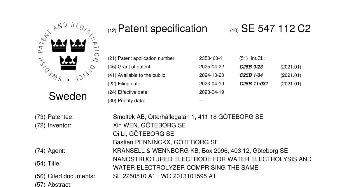
The Electrode Conformal Coating family offer a method for depositing conformally coated catalyst support for the PTL (porous transport layer) that provide both high catalytic activity and additional corrosion protection
Patents
October 9, 2024
The Electrolyzer Oxide Coating family offer a chemically stable solution, coating a nanostructure with non-noble metal oxides, this avoiding the use of expensive platinum for anode porous transport electrodes (PTEs). The inventions also improve the durability and efficiency of the PTE.
Patents
August 1, 2024
The Multilayer Cap patent family introduces a MIM-capacitor device that can double or triple the capacitance density of Smoltek's CNF-MIM capacitors. The patent details an invention for a layered energy storage device, specifically a capacitor, built using a metal-insulator-metal (MIM) configuration.
Patents
February 27, 2024
The Vertical Graphene family offer lowered contact resistance between separator elements and adjacent components in electrochemical cells and increase resistance to corrosion.
Patents
February 27, 2024
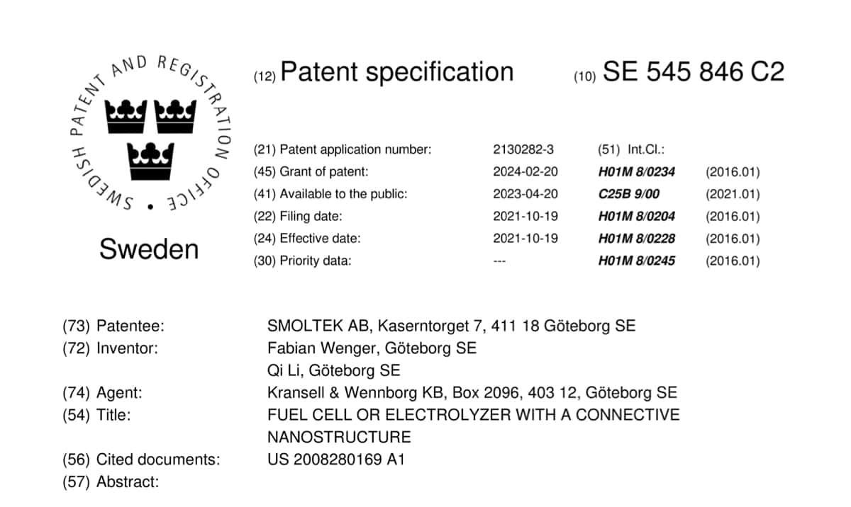
The Nano Velcro family improves the interlayer connections in electrochemical cells by using elongated nanostructures that are mechanically entangled between the layers.
Patents
February 27, 2024
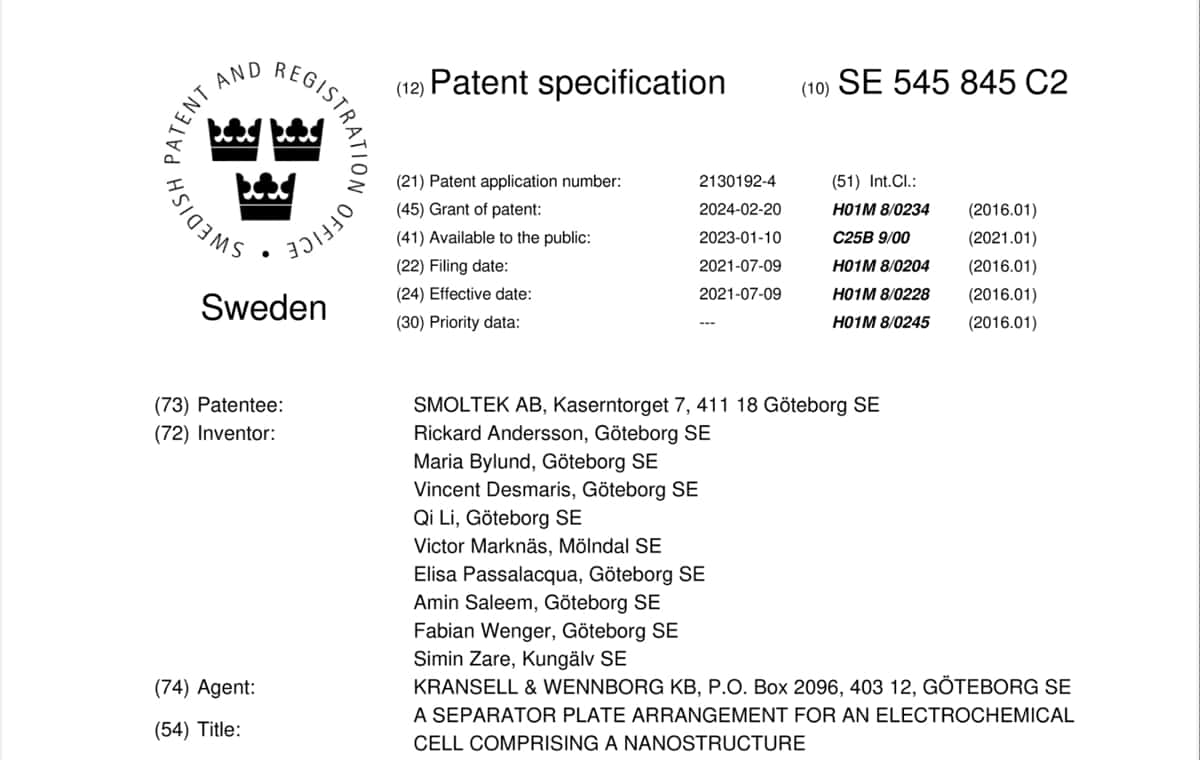
The Contact Resistance patent family is covering how to improve a separator plate arrangement for an electrochemical cell by comprising a nanostructure which offers lowered contact resistance between the separator element and the diffusion layer.
Patents
November 8, 2023
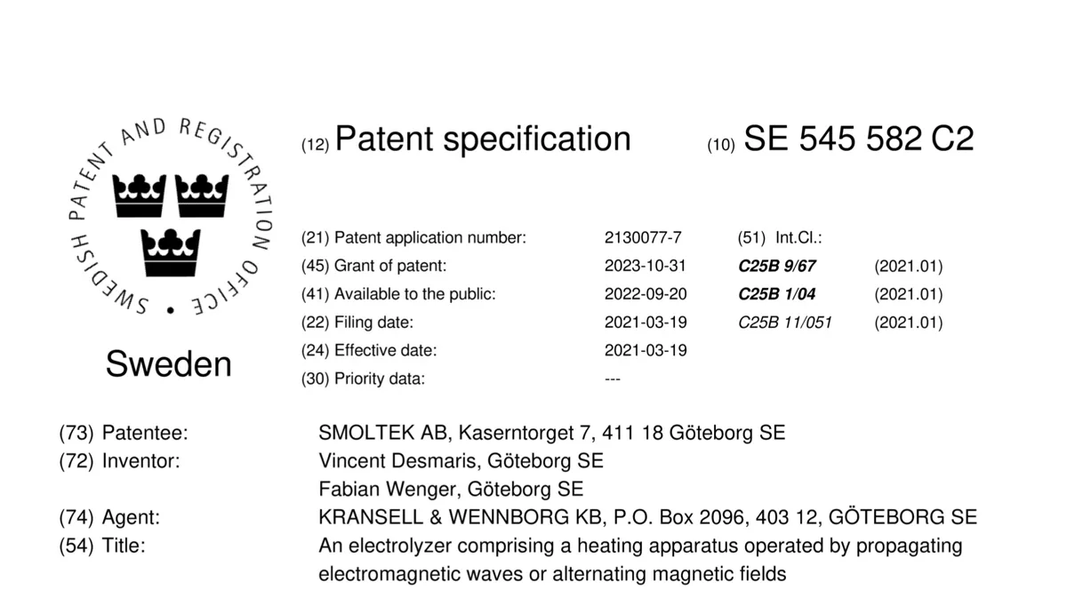
The Electro Catalyst Heating family is covering a way of arranging a temperature gradient in the electrolyzer by increasing a temperature of the catalyst structure. The innovation is targeted towards the production of green hydrogen using PEM electrolyzers.
Patents
August 18, 2023
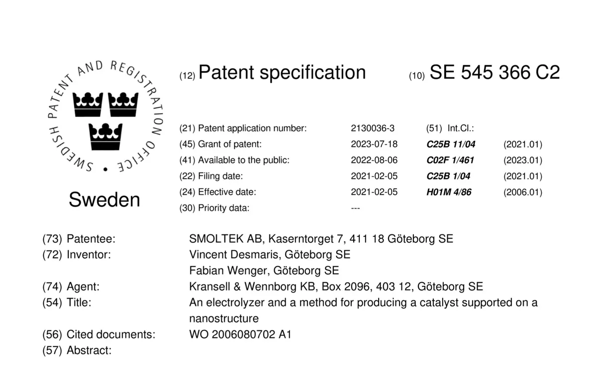
The Electro Catalyst Support family is covering an electrolyzer and a method for producing a catalyst supported on a nanostructure. The innovation is targeted towards the production of green hydrogen and discloses how carbon nanofibers can support the iridium catalyst load in a PEM-electrolyzer in a better way.
Patents
June 13, 2023
The Discrete CNF-MIM patent family is covering a method for manufacturing of discrete capacitor components based on our CNF-MIM technology. The innovation exploits the extra-ordinary surface to volume ratio provided by carbon nanofibers to create a MIM capacitor with unparalleled high capacitance density.
Patents
August 23, 2018
The Compact Energy Storage Interposer family is covering the invention and manufacturing of extremely thin energy storage devices embedded in an interposer.
Patents
May 3, 2017
The Assembly platform family is a particular application in the field of interconnects and heterogeneous integration.
Patents
February 24, 2017
The Interposer family is covering Smoltek's CNF-MIM capacitors technology and various use cases for the same, primarily in the field of interposers for advanced packaging and heterogenous integration of semiconductors.